When creating projects in KiCad it is often necessary to create symbols and footprints that are not a part of the KiCad standard library.
Prerequisites
- Basic Circuit Theory
- Baseline understanding of KiCad UI/Workflow
Creating Symbol Libraries
Creating symbol libraries is done from the Symbol Editor, which can be navigated into from the Schematic Editor or the KiCad project main page.
From the Schematic Editor: navigate to Tools -> Symbol Editor
From the KiCad Project Menu: click into “Symbol Editor” under “Schematic Editor”
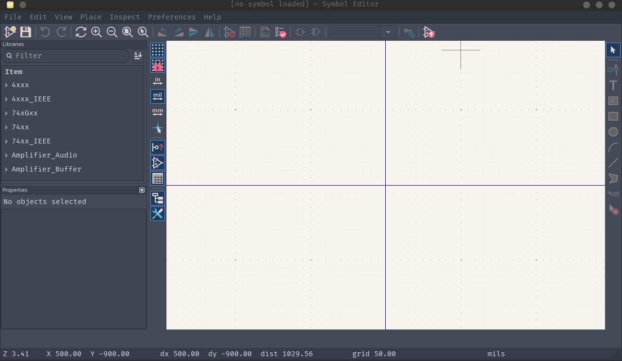
To create a new library, go to File -> New Library
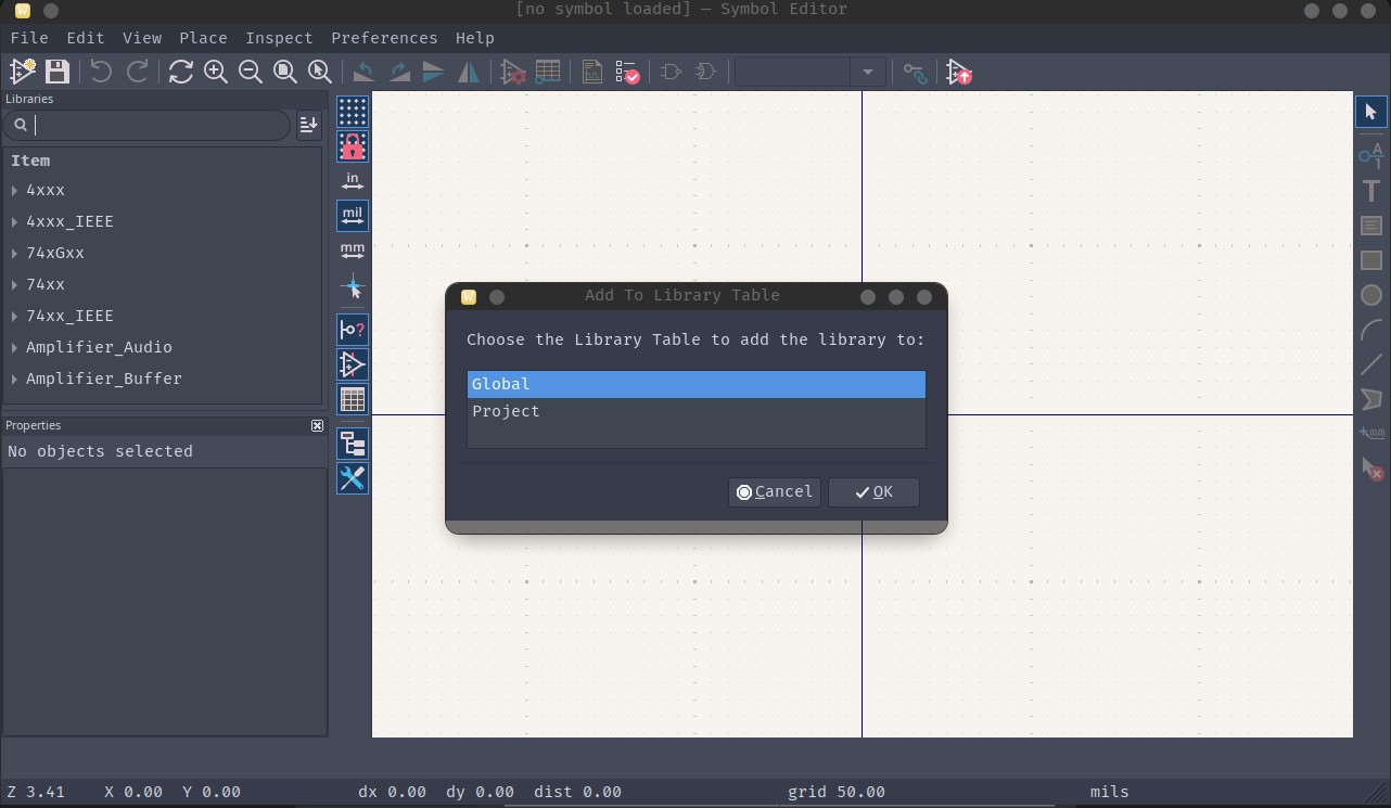
Global Libraries are available for any project that is done on the same system while Project libraries are only available in the current project. It is usually preferred to use Project Libraries over Global Libraries to maintain portability.
Find a location to place the kicad_sym file, which is your library. For project libraries it is recommended to place this file in a project local directory, Crab Labs usually places this in a “lib” folder in the project folder.
Once the library is created and placed, then symbols can be created and added to it.
Creating Custom Symbols
The Symbol Editor
All of this process will take place in the Symbol Editor, it is complex and feature rich.
On the right hand side there will be a toolbox, these are all of the tools that are available for use during the process
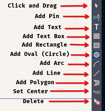
Once in the Symbol editor a new symbol can be created by using Command+N or Ctrl+N
Naming the Symbol
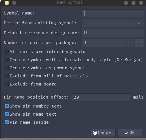
Name the symbol the name of the component you want to add. The reference designator must be added to indicate the type of component, these are standardized in IEC 60617 or IEEE Std 35:
- AT: Attenuator
- BR: Bridge rectifier
- BT: Battery
- C: Capacitor
- CN: Capacitor network
- D: Diode (including zeners, thyristors and LEDs)
- DL: Delay line
- DS: Display
- F: Fuse
- FB: or FEB Ferrite bead
- FD: Fiducial
- J: Jack connector (female)
- JP: Link (Jumper)
- K: Relay
- L: Inductor
- LS: Loudspeaker or buzzer
- M: Motor
- MK: Microphone
- MP: Mechanical part (including screws and fasteners)
- P: Plug connector (male)
- PS: Power supply
- Q: Transistor (all types)
- R: Resistor
- RN: Resistor network
- RT: Thermistor
- RV: Varistor
- S: Switch (all types, including push-buttons)
- T: Transformer
- TC: Thermocouple
- TUN: Tuner
- TP: Test point
- U: Integrated circuit
- V: Vacuum Tube
- VR: Variable Resistor (potentiometer or rheostat)
- X: Transducer not matching any other category
- Y: Crystal or oscillator
- Z: Zener Diode
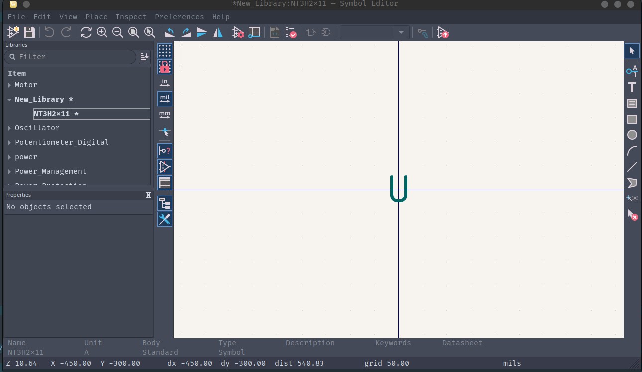
Once that has been done it will look like this:
Defining the Symbol Shape
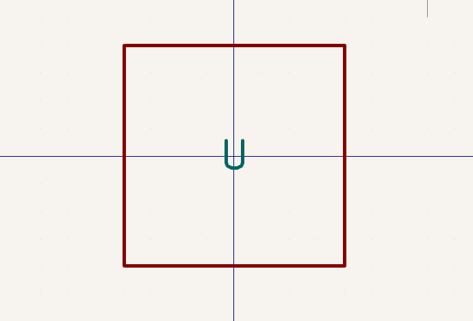
The first step in creating a symbol is defining the shape or the outline of the symbol, you can use any of the polygon tools or the oval tools to draw a shape in which to add pins to. This can be any shape but rectangular bodies are generally standard.
Adding Pins
The next step is to add the pins, if there are a lot of pins the body shape may need to be changed in order to be appropriately sized for the number of pins.
There are a number of different pin types in KiCad:
- Power Input: This pin receives power from an external source (e.g. a VDD pin on a micro controller)
- Power Output: This pin supplies power to an external sink (e.g. VIN pin on a DC Jack)
- Input: This pin receives digital signals from an external source (e.g. Reset pin on an MCU)
- Output: This pin sends digital signals to an external sink (e.g. Status pin on an MCU)
- Bidirectional: This pin sends and receives digital signals (e.g. USB D+ and D- pins on an MCU)
- Tri-State: This pin can be input, output, or high-Z (floating) (e.g. GPIO in general)
- Passive: This pin does not strongly interact with anything (e.g. A pin on a resistor)
- Free: This pin is floating (e.g. Extraneous pins)
- Unspecified: It is not known what this pin does
- Open Collector: This pin needs a pull up resistor to operate correctly (e.g. SDA and SCL on I2C)
- Open Emitter: This pin needs a pull down resistor to operate correctly
- Unconnected: This pin should not be connected to anything (e.g. Some thermal pads)
For every pin in your symbol, the type must be defined. These definitions help KiCad figure out how the design fits together. These definitions allow for ERC (Electrical Rules Checking) to check the connection logic of your circuitry, which catches errors early.
It is important to check the data sheet for this information about the pins of the device you are designing the symbol for. The data sheet will include the pin number for all of the pins, use this in creating the pins.
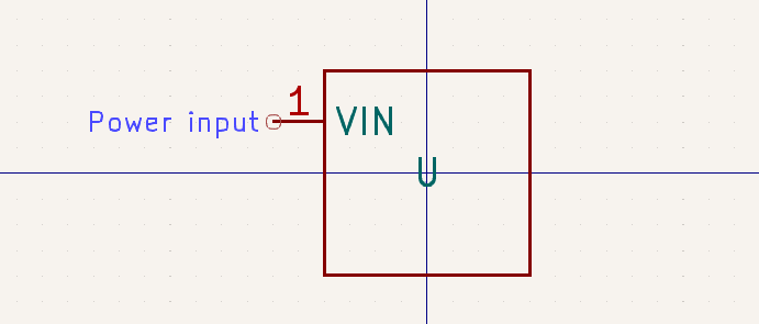
Once you have created a Pin, move it and rotate it (using “R”) so that the pin name is inside of the design:
Crab Labs highly recommends following these pin placement guidelines:
- All Input Power (VCC, VDD, VIN, etc) should be either on the top of the symbol or the left side
- All Ground (VSS, VEE, GND, etc) should be either on the bottom or the left side of the symbol
- All Inputs should be on the left side of the symbol
- All Outputs should on the right side of the symbol (this includes power outputs)
- Pins should be organized logically rather than numerically (i.e. put related pins next to each other)
- Pins should be separated by class (i.e. put extra spacing between groups of related pins)
If these guidelines are followed, symbols should be easier to parse as well as to work with in the schematic.
Once you have defined and placed all your pins, you should modify the symbol properties. This can be done by pressing “E” while not selecting anything in the Symbol Editor
Defining Symbol Properties
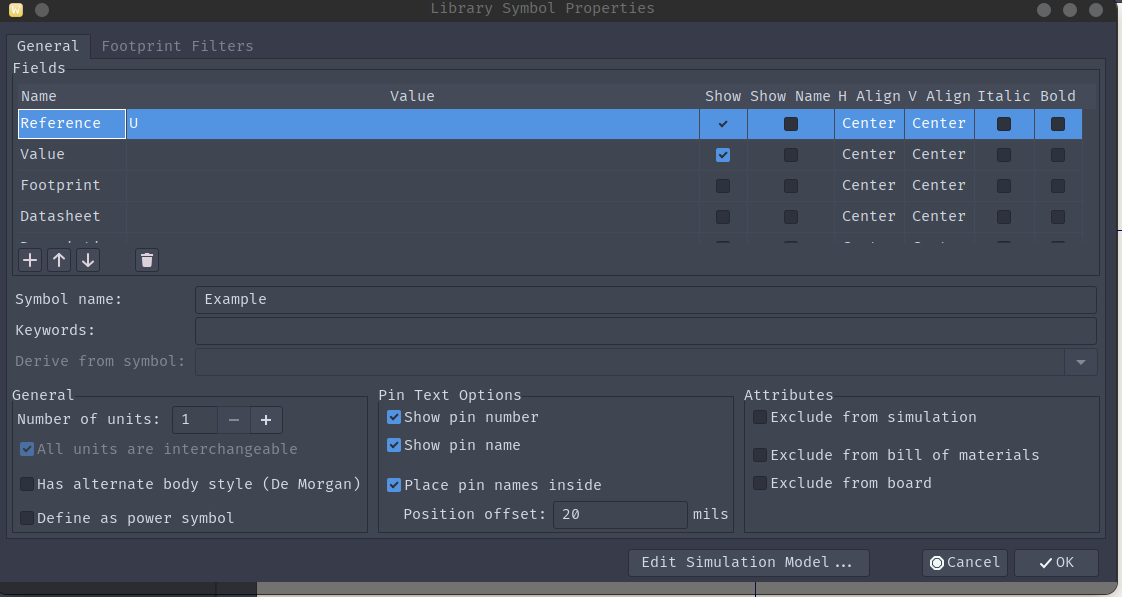
It is recommended to insert the name in value field, a link to the datasheet in the datasheet field, a small description in the description field, as well as the footprint if it is fixed and exists.

Once the symbol fields are defined and the symbol has been cross checked against the data sheet, then the finishing touches should be applied.
Finishing Symbols
Apply coloring to the symbol by clicking the outline polygon and pressing “E”
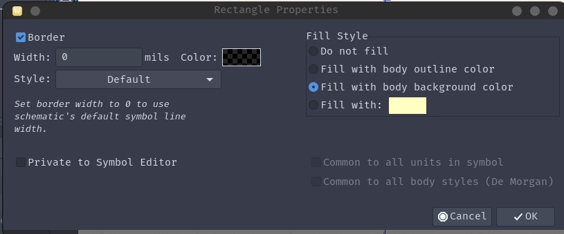
The default coloring for KiCad symbols is “Fill With Body Background Colors”. This is recommended in most cases.
Once the coloring is set, then press “Ctrl+S” or “Command+S” to save the symbol into a library.
Custom Symbol Example
A symbol will be created for a new component, the NT3H2 NFC Tag by NXP. Looking at the datasheet we can find a pin-out diagram for the available packages, I will be picking the TSSOP-8 Package at random.

Paired with the pin description we can begin to create a symbol for it.
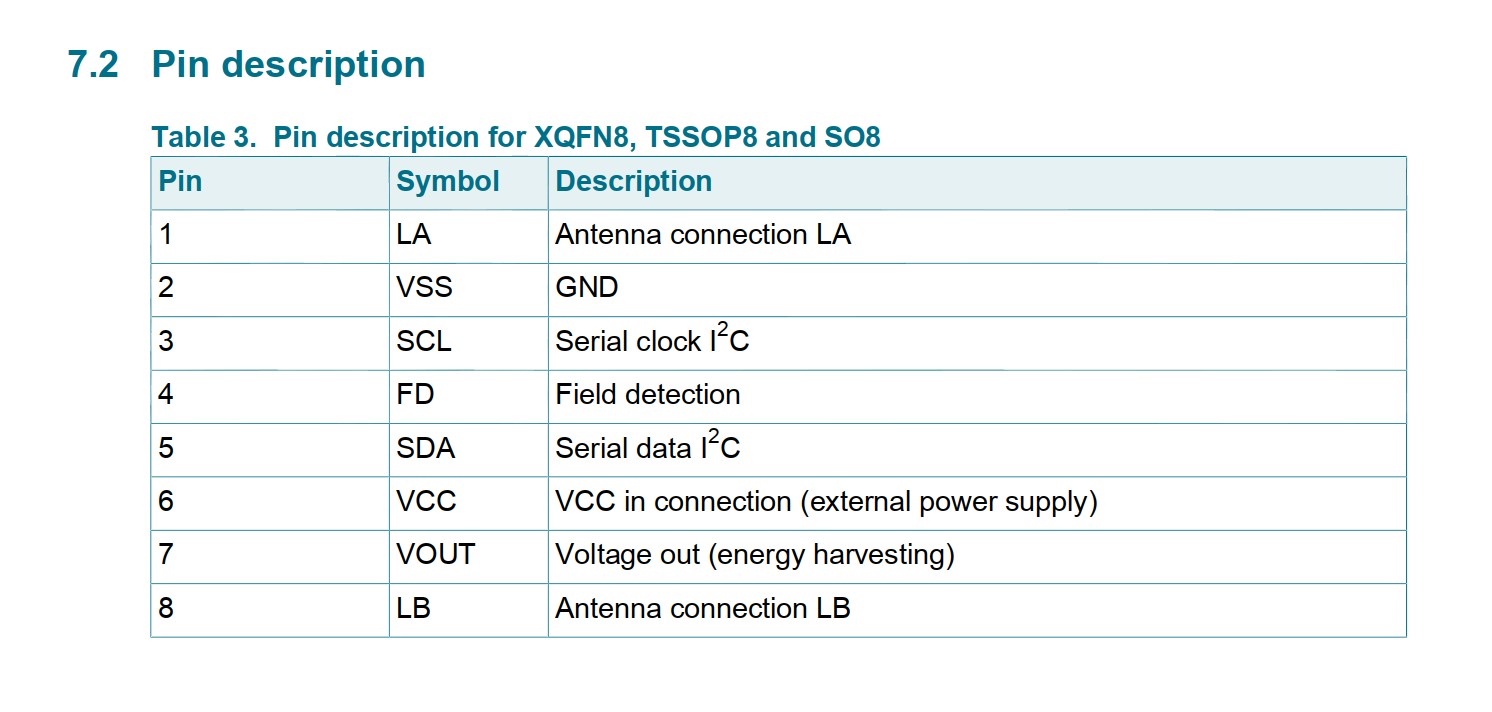
We see that the pin-out is the same (same pin number has same function) across all packages. This mean that this symbol can be used for any of the different footprints.
A symbol is created with the name “NT3H2x11” which reflects full name of the chip, the x represents the different variants with different memory

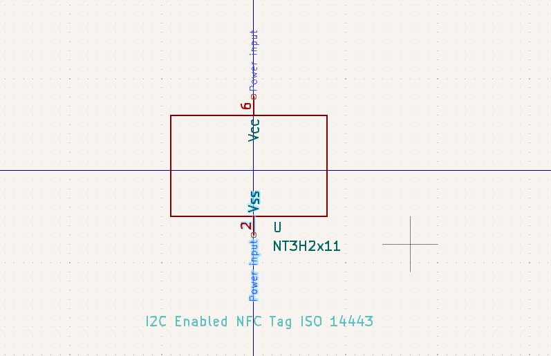
The symbol properties will be modifed to include information about the component and the pins will be added. First to be added is VCC (Pin 6, Power Input), next is VSS (Pin 2, Power Input), these are both provided power from some other source, so they are inputs.
Next to be added are the I2C pins (SDA and SCL), these are bi-directional but could also be open collector
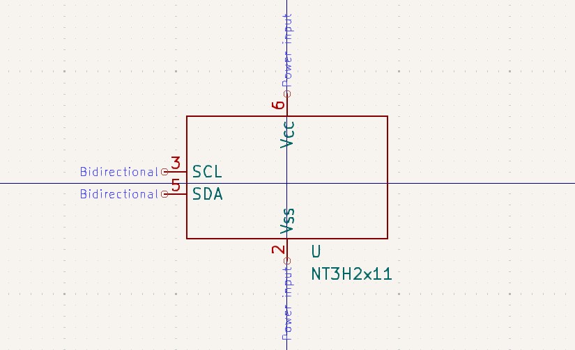
After that, the RF circuitry needs to be added (FD, LA, LB, and VOUT). LA and LB are passive since they are analog signals, FD is Open-Drain (Open Collector), and VOUT is Power Output.
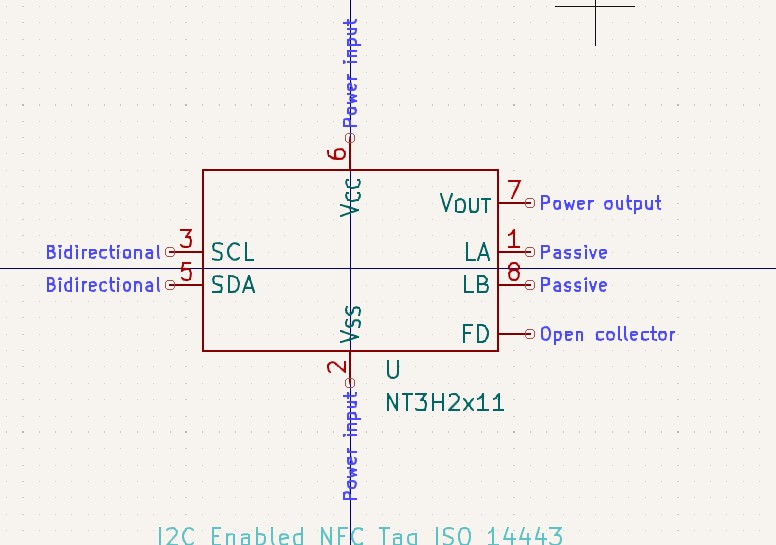
Now we fix the coloration of the rectangle:
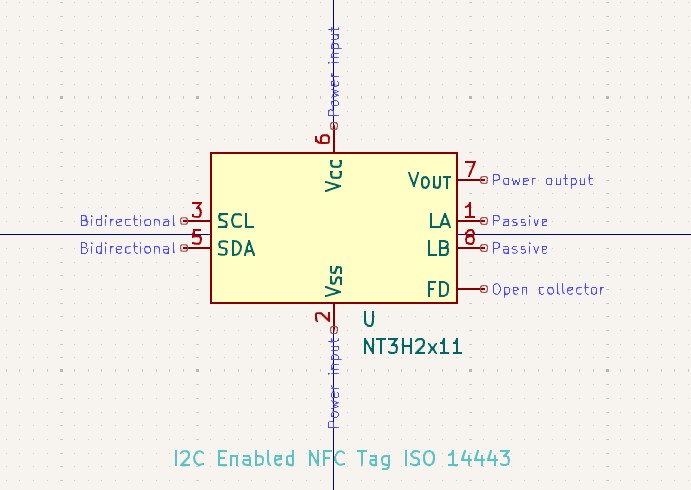
We can then save the symbol and use it in a project.
Creating Footprint Libraries
The process for creating custom footprint libraries is almost identical to the process for creating symbol libraries.
From the KiCad main menu open “Footprint Editor” or from the PCB Editor go to Tools -> Footprint Editor
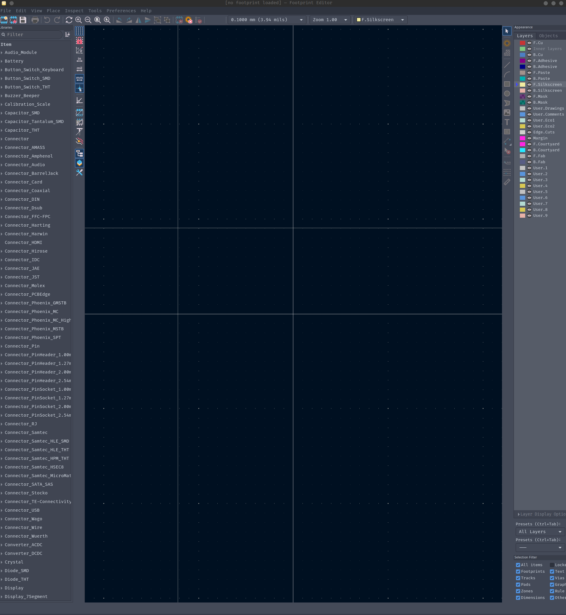
To create a new library navigate to File -> New Library
Global Libraries are available for any projects on that device, Project Libraries are only available for the current loaded project. It is recommended to use Project Libraries by default.
This will create a folder called *.pretty, name it appropriately and find a place to put it. For Project specific libraries, Crab Labs strongly recommends naming them the same as the project and placing them in a “lib” folder in the project root.
Creating Custom Footprints
Primer on Footprint Types
There are two major types of footprints:
- SMD: Surface mount devices, these footprints do not have any mounting holes (i.e. components with these footprints are fully contained on one side of the board)
- THT: Through hole technology, these footprints have pins or mounting that extend through the board (i.e. these components are soldered on the opposite side they are placed)
Generally most components now days are SMD but there are still lots of components that need to be THT.
Looking at the data sheet for your device, there will be a section that details the footprint. If there are holes in that drawing then make a THT component, else make a SMD component
The Footprint Editor
The footprint editor is a complex interface, the basic available tools are shown here:
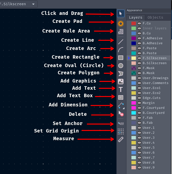
These tools interact and are used with these layers
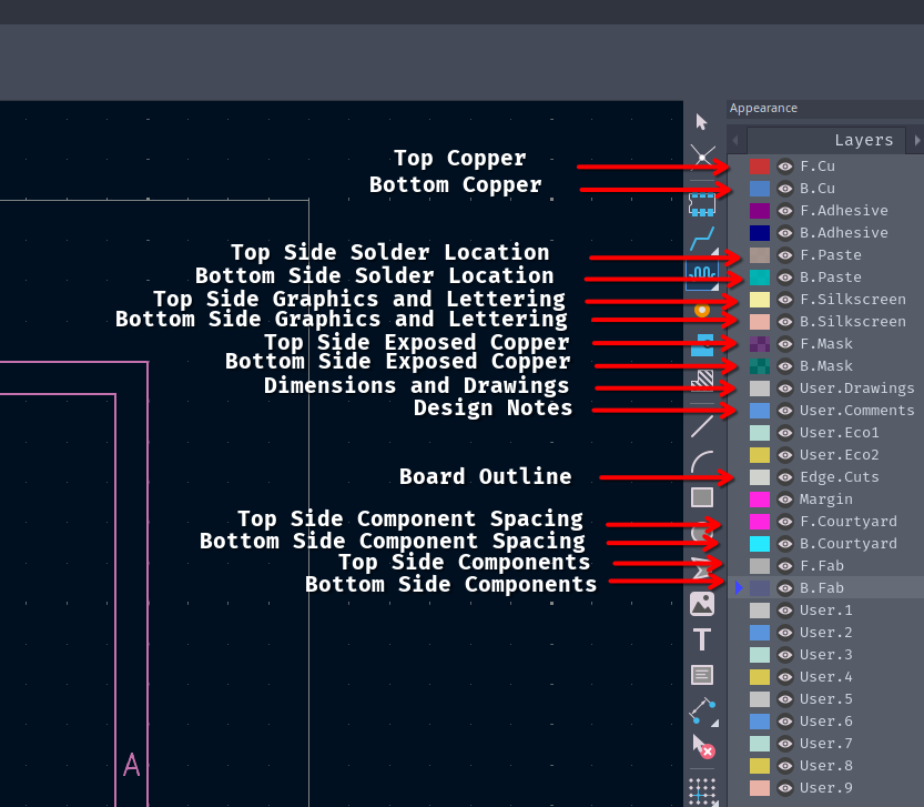
Using the Footprint Wizard
The easiest way to create custom footprints with KiCad is by using the Footprint Wizard.
The footprint wizard can be limited and does not cover all possible packages. If your component is not a standardized form factor then manual footprint creation is the only option, go here.
The footprint wizard can be used by navigating to File -> Create Footprint
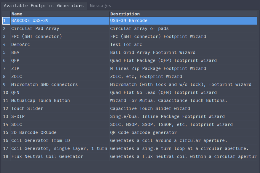
The footprint wizard can create the following types of footprints by default:
- Barcode: This is just the same as a barcode in the grocery store
- Circular Array of Pads: Exactly what it sounds like (somewhat common for old transistors and amplifiers)
- FPC: Flat Panel Cable Creates footprints for SMD connectors to flexible cabling
- BGA: Ball Grid Array, High density footprint with very small circular pads in a grid
- ZIP: Zig-Zap Inline Package, THT footprint type often used by older computer chips
- QFP: Quad Flat Package, SMD footprint with pads that protrude on all four sides
- ZOIC: SMD version of ZIP
- MicroMatch: Creates footprints for female MicroMatch connectors
- QFN: Quad Flat No-Lead: SMD footprint with pads that do not protrude with often a large pad in the middle
- Mutual Cap TouchButton: Generates capacitive touch sensing buttons
- Touch Slider: Generates a touch sensitive slider that can detect touch point
- S-DIP: Single or Dual Inline Package: THT footprint for components with through hole pins on one or two sides of the package
- SOIC: Small Outline Integrated Circuit, SMD footprint with protruding pads on two sides of the body
Click on the desired footprint type and the wizard will ask for all relevant parameters
Using this to generate an SOIC footprint would look like this:
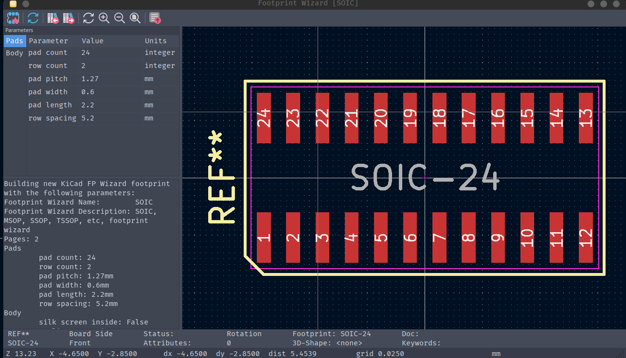
These parameters can be seen in the datasheet, such as is seen here:
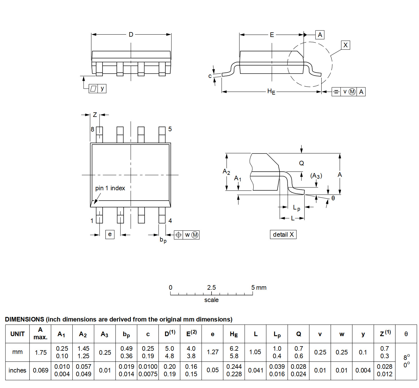
Applying these dimensions to the wizard leads to the following footprint:
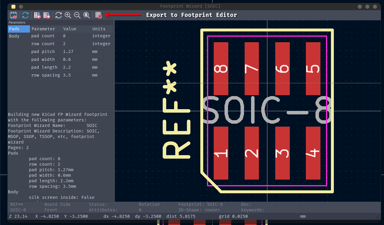
Once the dimensions are entered, then the footprint should be exported to the Footprint Editor using the button highlighted
Once in the Footprint editor the last steps will match that of a manually created footprint, see here
Manual Footprint Creation
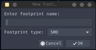
To create a footprint within the footprint editor select the library which shall contain the footprint and press “Ctrl+N” or “Command+N”
Looking at the data sheet for your device, there will be a section that details the footprint. If there are holes for pads in that drawing then make a THT component, else make a SMD component
If you are unsure of the component type or the component is non-electrical make it “Other”
Find the drawing of the footprint you are trying to recreate in the data sheet, it will likely be near the end of the data sheet and look similar to this:
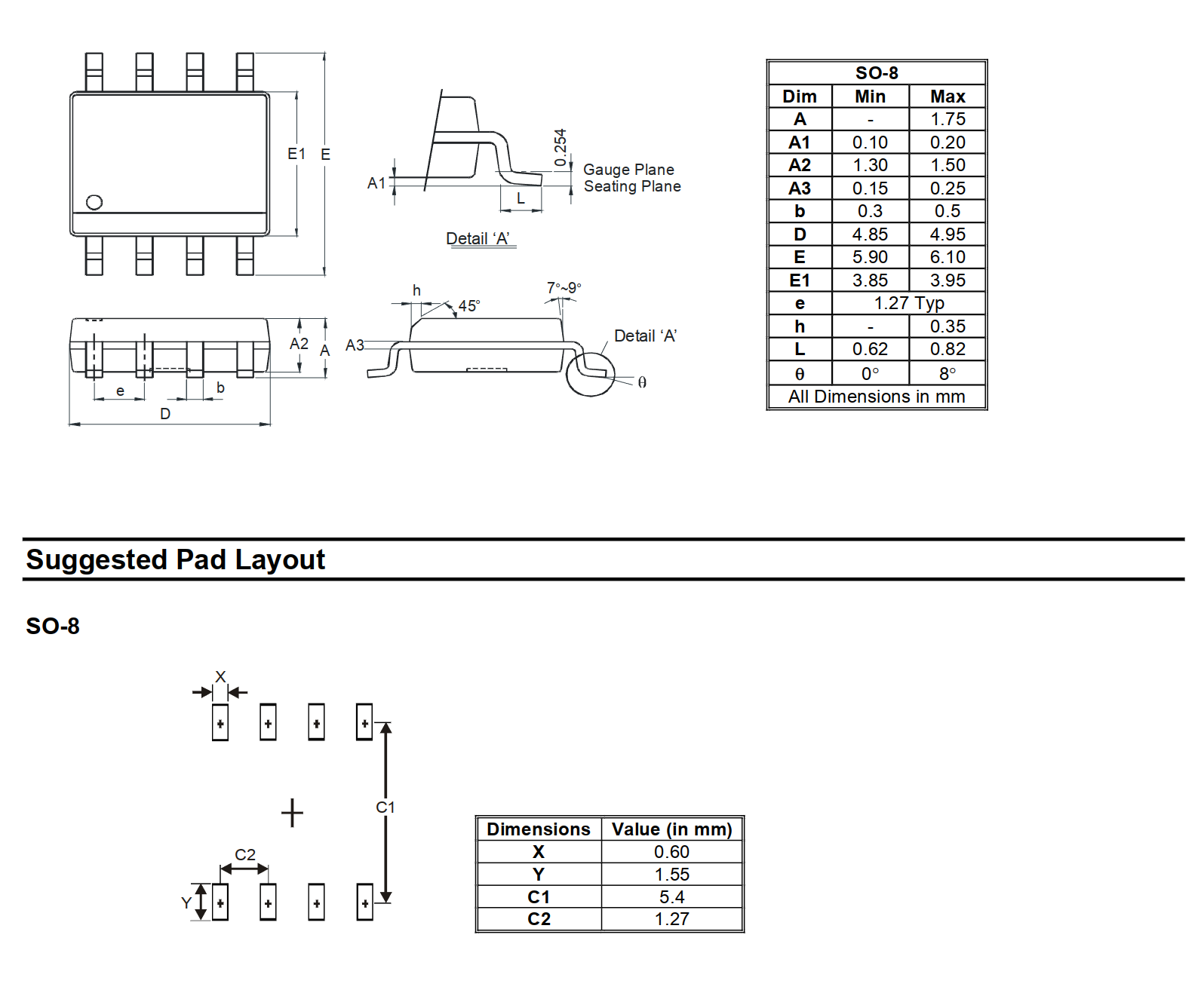
From the drawing we can derive the proper pad dimensions, there may be more than one different pad shape; be careful when reading.
Creating Pads
From the drawing we can see that a pad is recommended to be .6mm x 1.55mm, in order to set the pad size to that we need to use the “Pad Properties” menu. This can be accessed via Edit -> Default Pad Properties or via the shortcut located here:
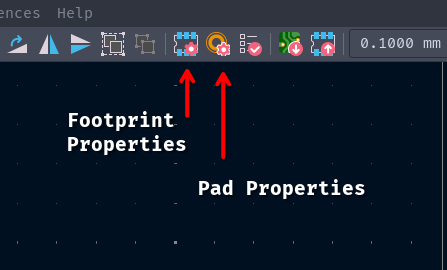
The menu looks something like this:
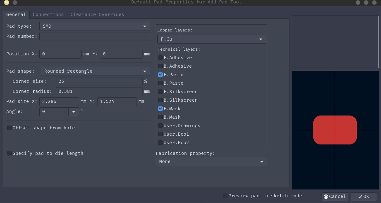
We can set the pad size to the desired value from the drawing:
For THT pads you would specify the pad as THT and define the hole shape and size along with the pad
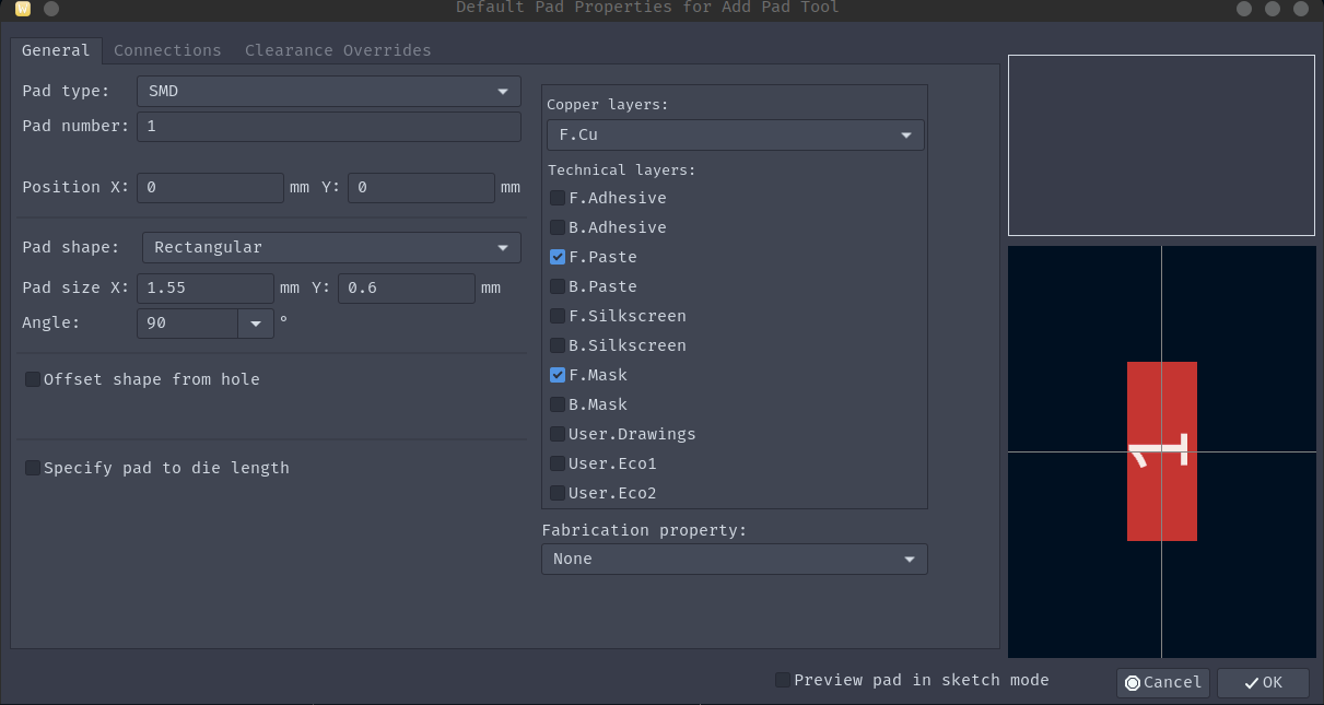
Then we can press Ok to leave this menu and start placing the footprints.
Placing Pads
To place a pad, use the “Create Pad” tool as seen here
It is important to place the pads according to the datasheet, adjusting the grid can make this much easier. The grid can be adjusted via a drop down menu shown here:
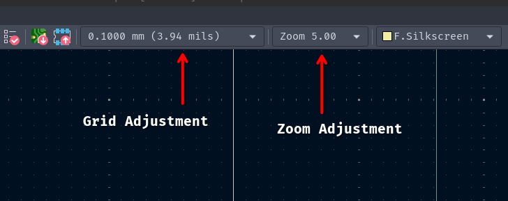
It is recommended to adjust the grid throughout the process to ensure proper placement of the pads. Objects snap to the grid which makes designing much easier.
For this footprint, a grid of 1.27 mm will be good to place the footprints in each row, and then another grid of .1 mm to space them apart from each other, followed by a grid of .635 to center the footprint
Creating and spacing the pads out with a 1.27 mm grid we get this:
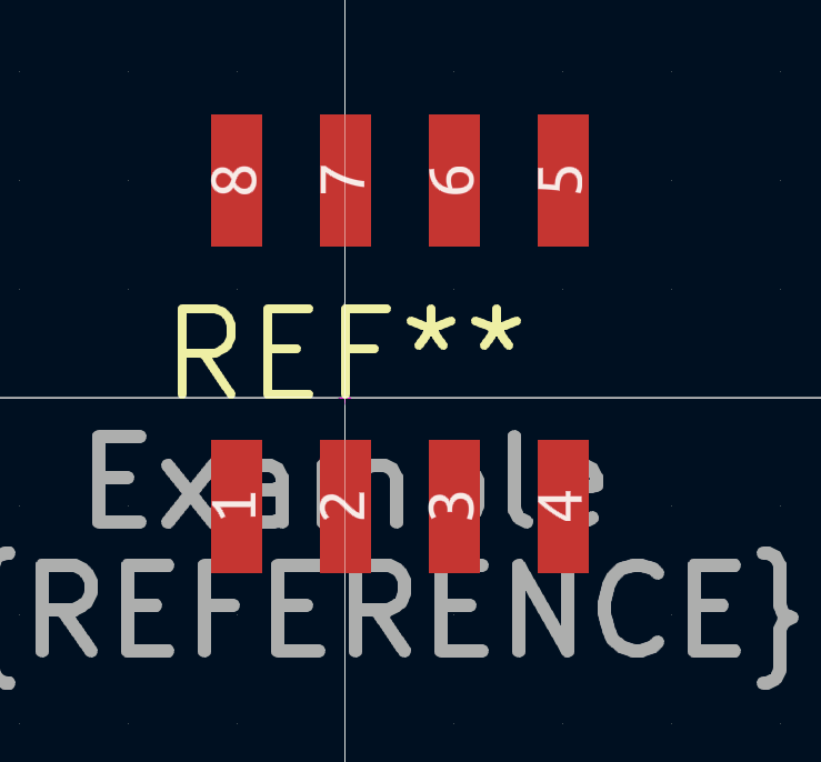
We then want to move each row to be 2.7 mm from the Y-Axis, we will use the change the grid to .1 mm and select all of the pads in a row. Once the pads are selected we can move them by pressing “M” and using the arrow keys or the mouse, the arrow keys are preferred for accuracy.
You can see the current cursor location on the bottom of the screen, as seen here:

This information should be used to ensure proper placement of the pads
Using the cursor location and an appropriate grid we can place the rows relative to one another
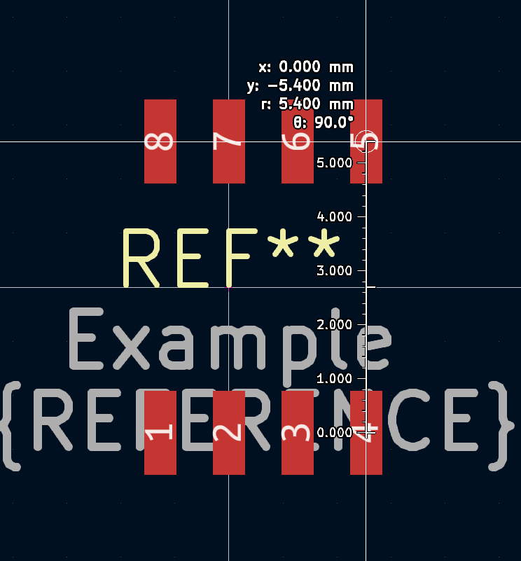
This uses the measure tool to check and show the distance, it is recommended to use this tool often to check spacing between pads and other elements
Adjusting the grid again we can then center the footprint in the X direction:
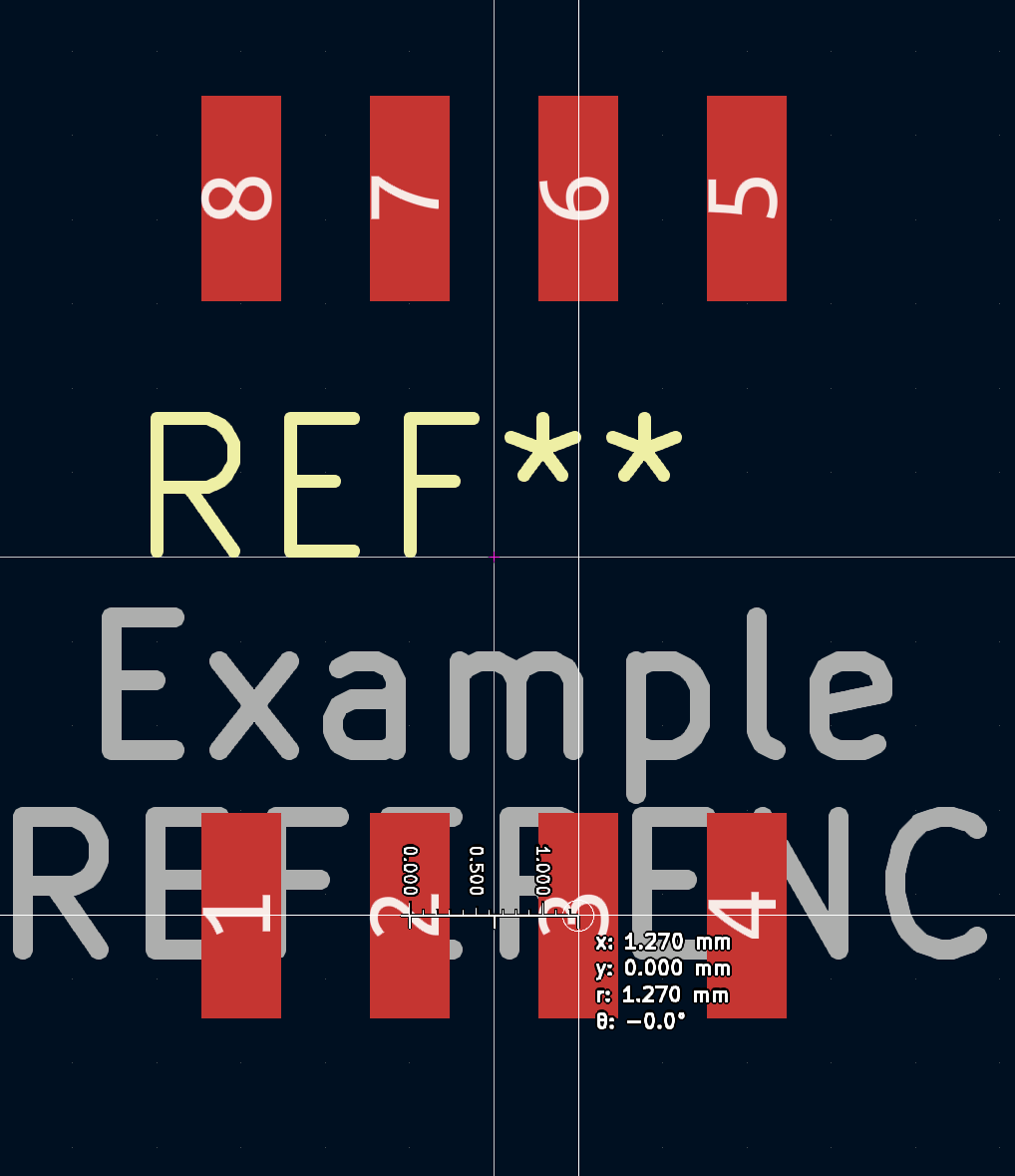
These are properly placed pads.
It is important to reference the datasheet to check for pin numbering
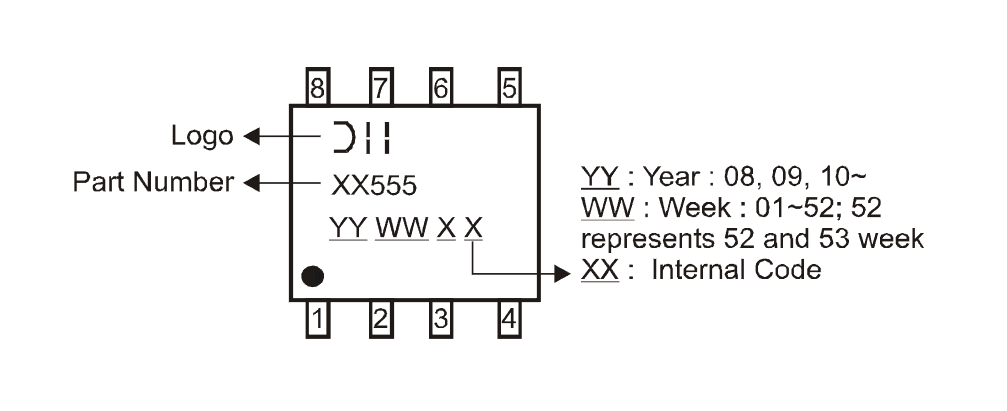
We can see that the numbering matches the numbering on the footprint, so we can proceed
Adding Finishing Touches
Before a footprint can be used in production there are a number of recommended tweaks and finishing touches that must be done
The first thing that should be done is defining the component in the Fabrication Layers (Fabrication Layers describe the size, shape, and value of components on the board)
To do this in the footprint editor we want to select the Fabrication Layer and draw the shape of the component. To do this click the Layer titled “F.Fab”, this represents the layers on the front (top) of the board.
Use the drawings of the component in the datasheet to determine the component dimensions
Once the layer is selected, use one or more of the graphics tools (Rectangle, Line, Polygon, Arc) to draw the shape of the component where it should be on the F.Fab layer, like this:
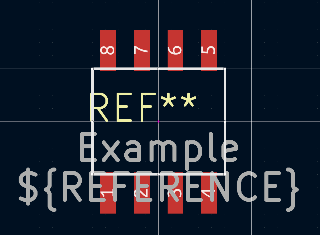
Once the Fabrication Layer has been drawn the next step is to draw the Courtyard.
The Courtyard is the area around a part which can’t have any other parts within. Courtyards generally are an outline of the component as well as the pads with a fixed offset.
A courtyard looks something like this:
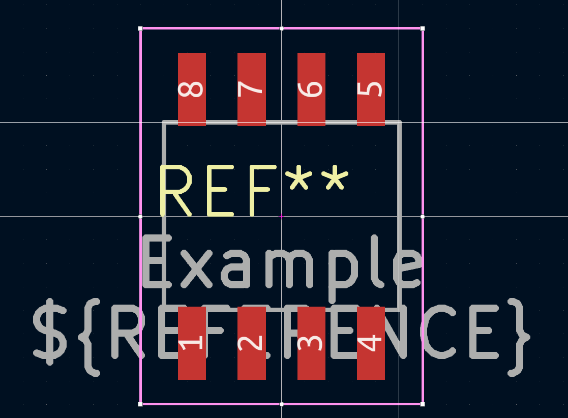
Click in to the F.SilkScreen layer and use the graphics tools to draw an indicator of orientation of the component body. The default indicator is a marker on Pin 1 of the device. KiCad has changed the default indicator from a small dot to a triangle.
Additional graphics can and should be added to show the component body and the like, here is a good example:
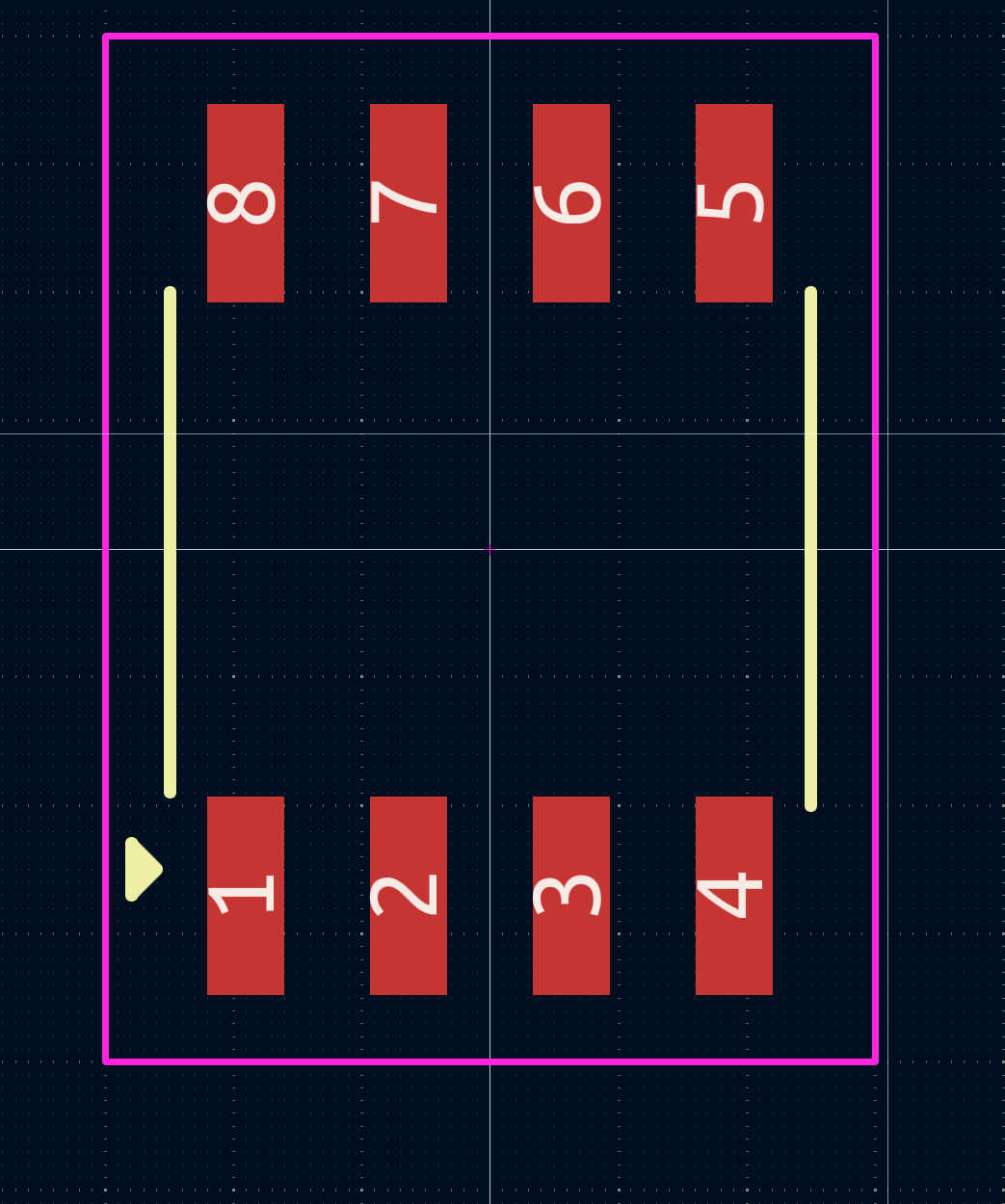
The triangle was drawn with the polygon tool and the lines were drawn with the Line tool.
After the Silkscreen has been added, the next step is adding Dimensions. This will take place in the User.Drawings layer and will utilize the “Add Dimension” tool.
Click in to the User.Drawings tool and use the dimensioning tool to show proper dimensions, like this:
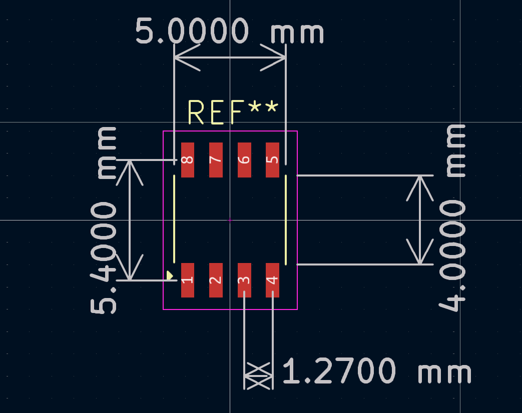
If you want to add additional notes or information include it in the User.Comments Layer
Finalizing Footprint
The last step in finalizing a footprint is modifying the footprint properties.
To edit the footprint properties, press “E” when not selecting anything in the Footprint Editor
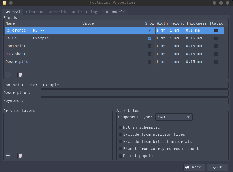
If the footprint is specific to a single component, then change the value to the exact component name, otherwise name it according to the datasheet’s name for it.
If there a 3-D model for the component, copy it to a project local location (Crab Labs recommends in a models folder in the lib directory). From the property menu click in to the 3-D Model tab:
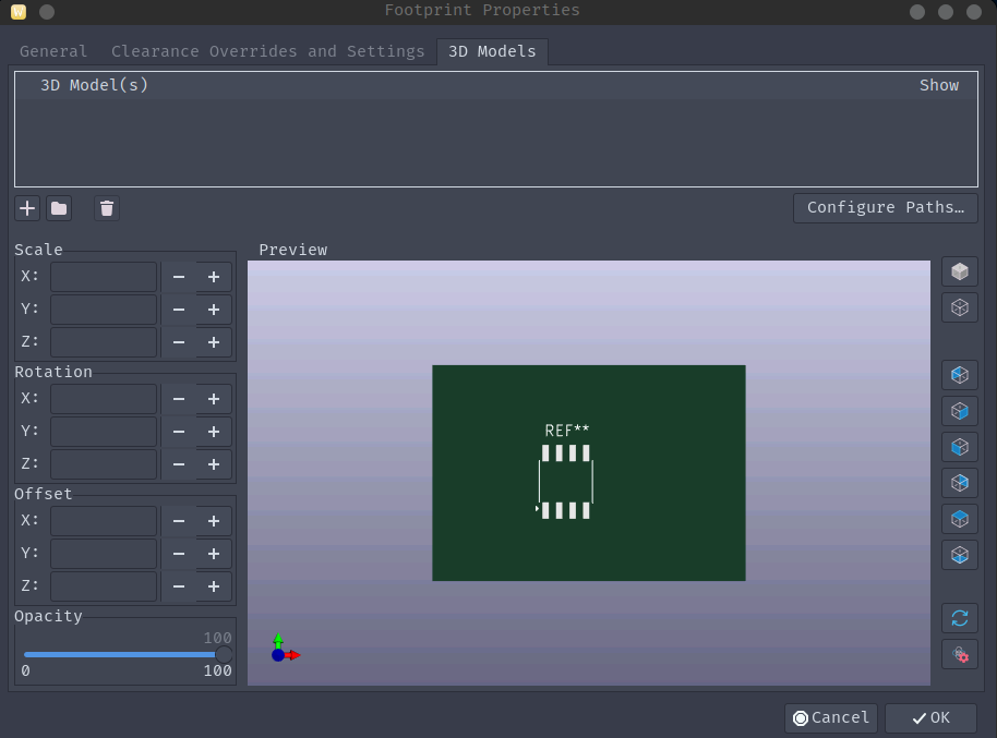
Click the file icon and find the location of the 3D model
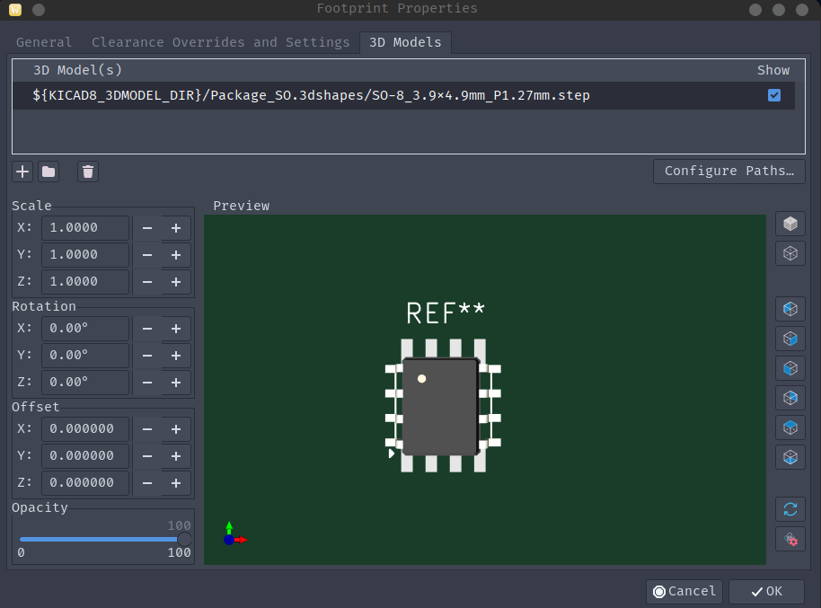
If the model is off axis or oriented incorrectly, it can be corrected via the adjustment menu on the left side. Once the model is oriented correctly it will look like this:
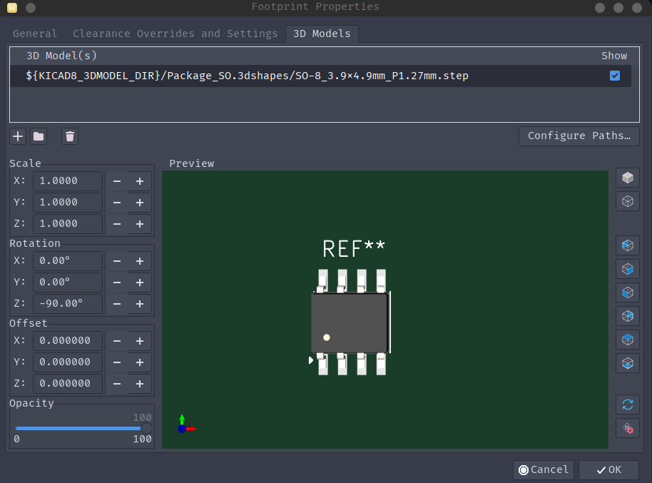
Once all of the properties are finalized then the footprint is ready to be used in your projects.
Custom Footprint Example
Lets say we need to creating a board with the NT3H2x11, an NFC Tag IC. There is a footprint available online, but I will be showing how to make the footprint from scratch. After viewing the datasheet, the only form factor that would work in the design is this:
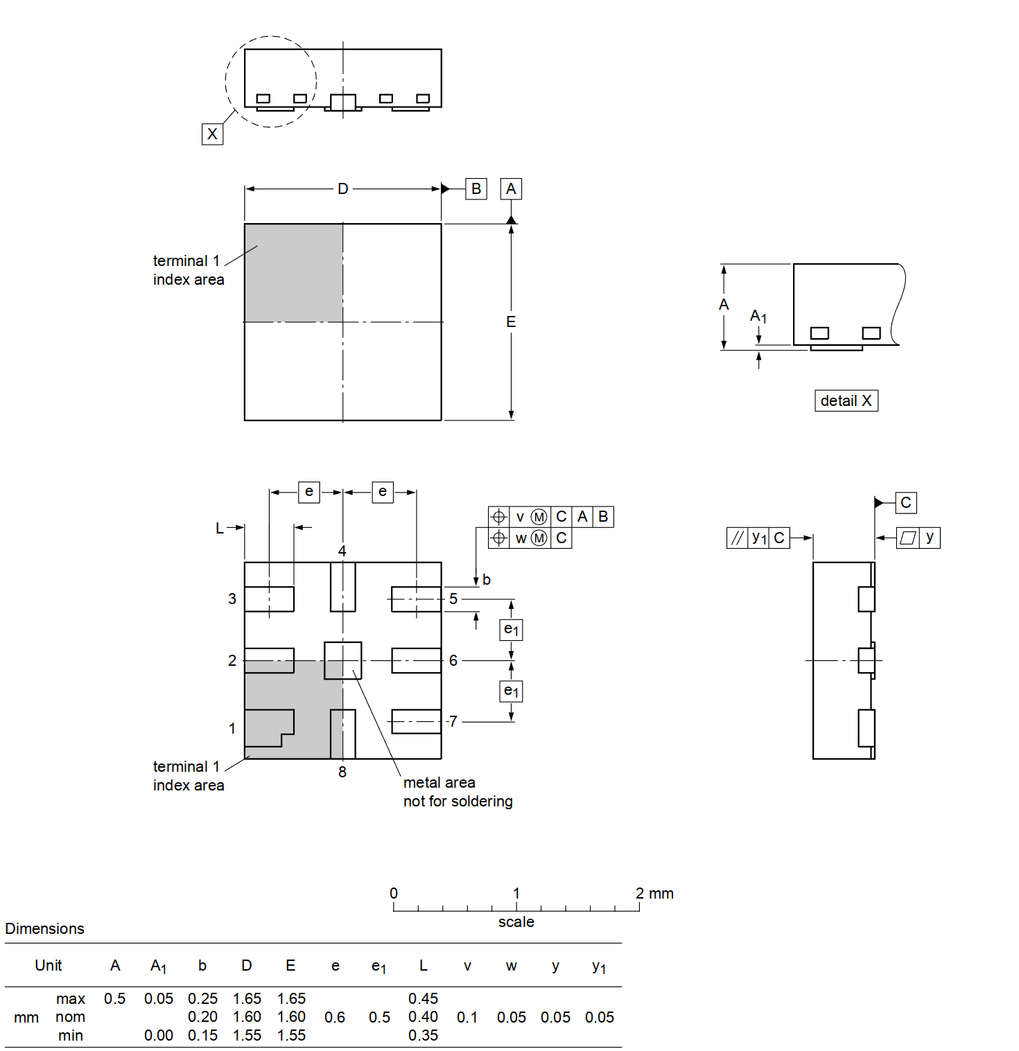
This is in no way standard nor is it in the KiCad standard library.
First thing is to create a library is there isn’t one already
After the library is created we want to create an empty footprint, we will can it XQFN8, the name stated on the datasheet
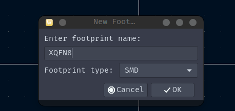
Now we want to look at the datasheet and define the size of the pads:
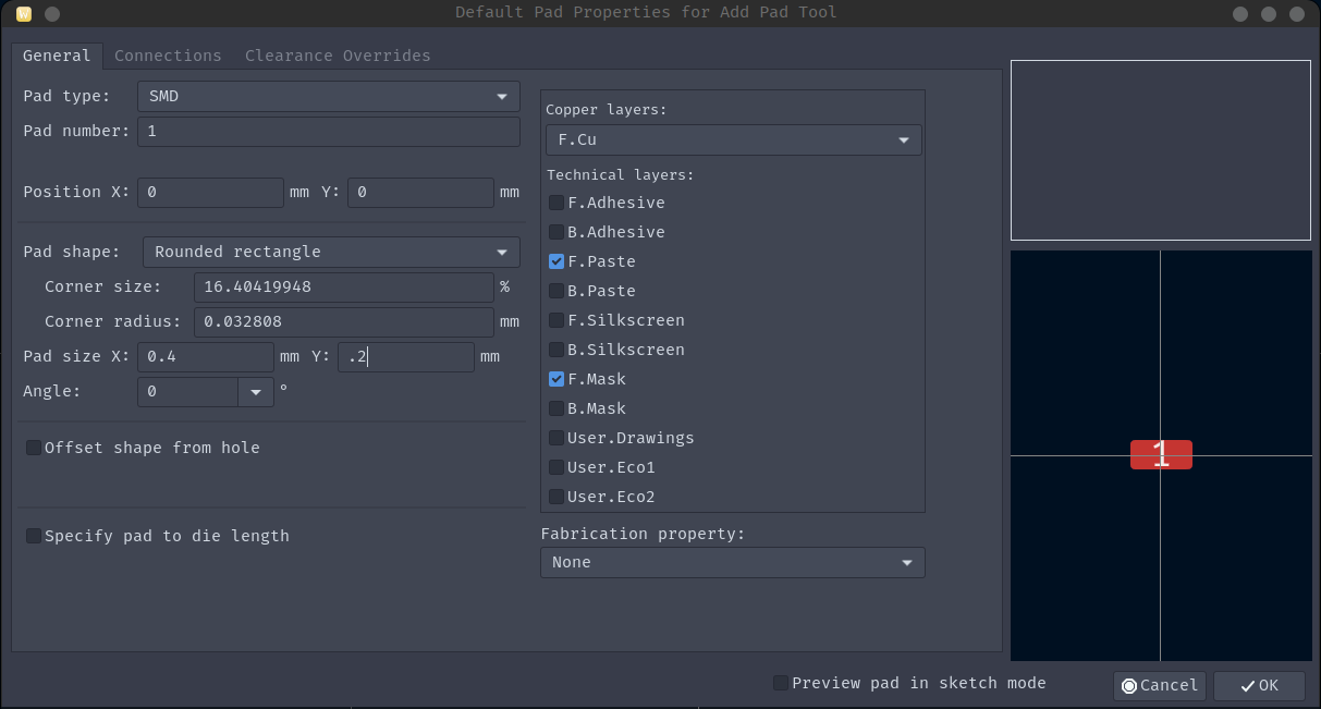
Then we want to place the first pads using the spacing provided in the datasheet and add the rest of the pads roughly where they need to be:
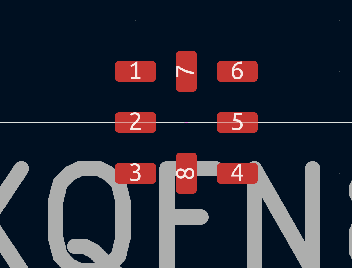
We then need to fix the pin numbering, we enter in to the pad properties by pressing “E” on a pad and modifying the pad number:
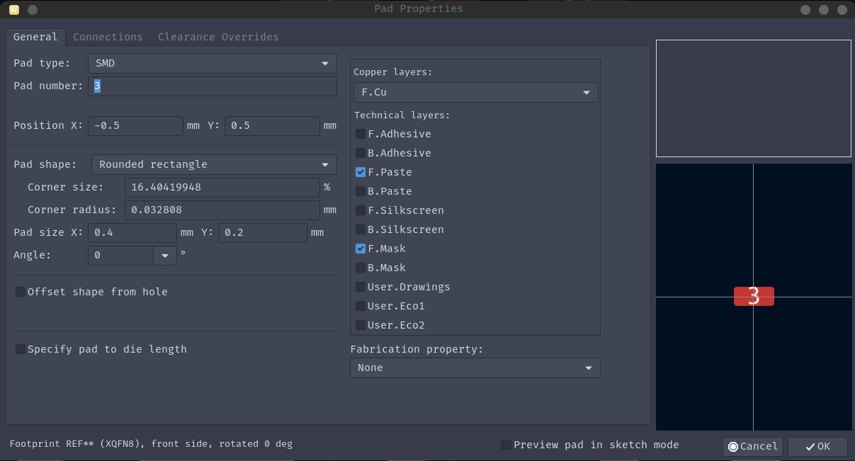
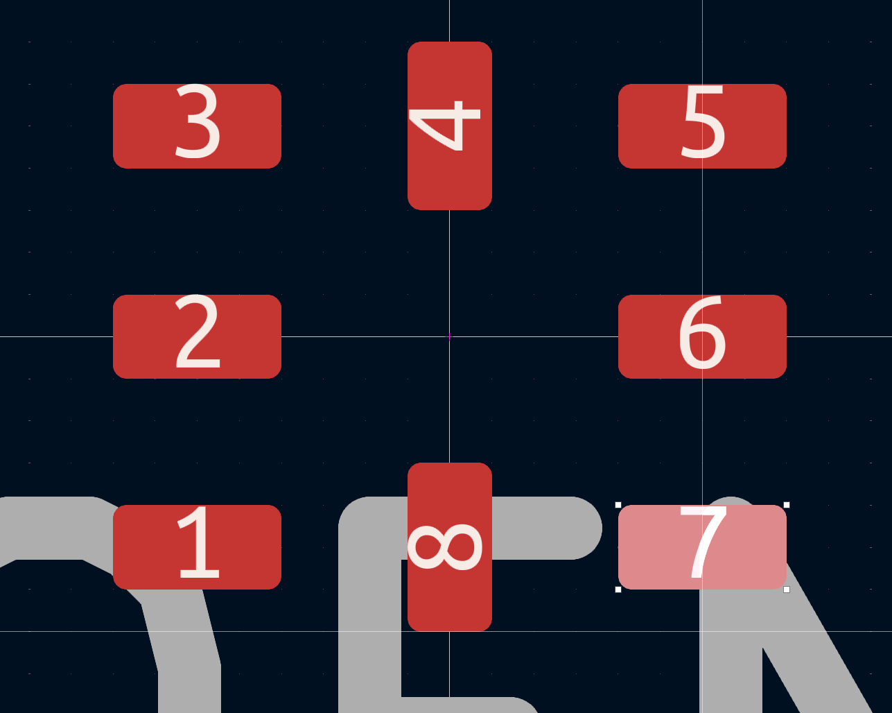
Once the numbering is fixed we need to move the pins in to the proper location according to the datasheet
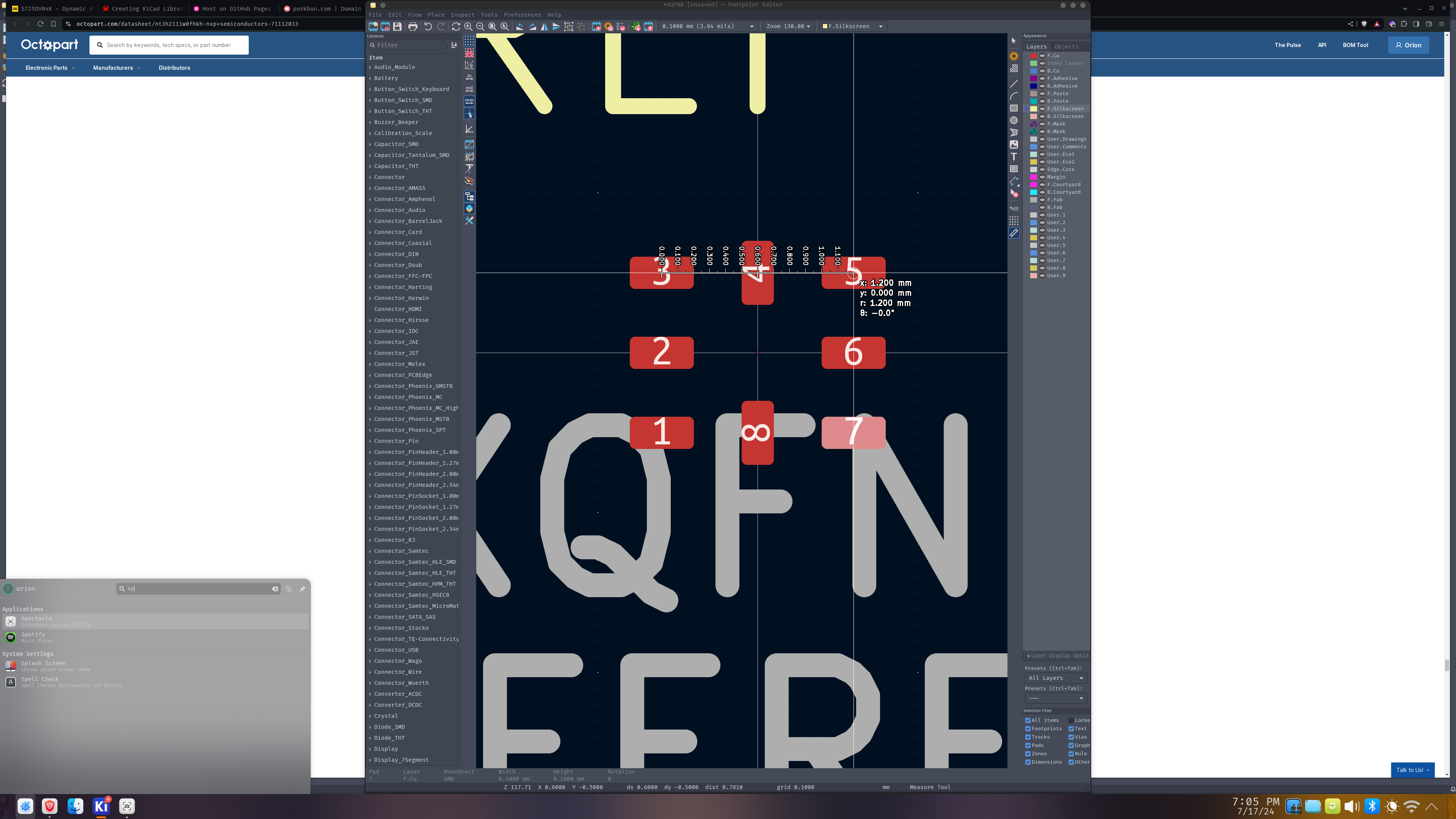
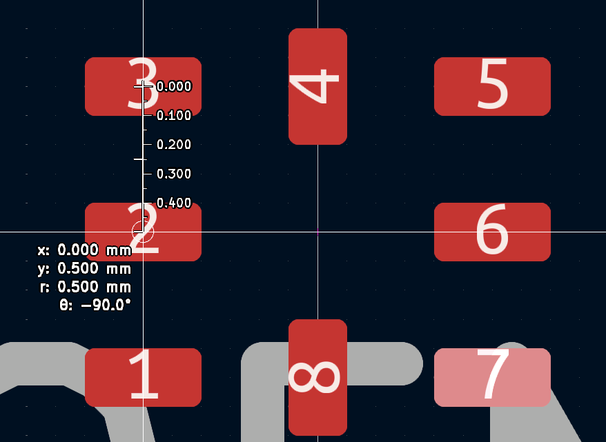
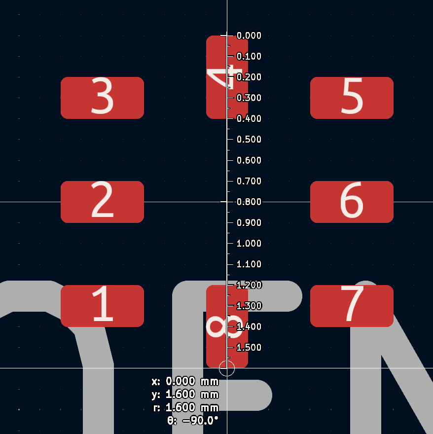
Now that the pads are properly placed let’s add a fabrication indicator to show the component outline
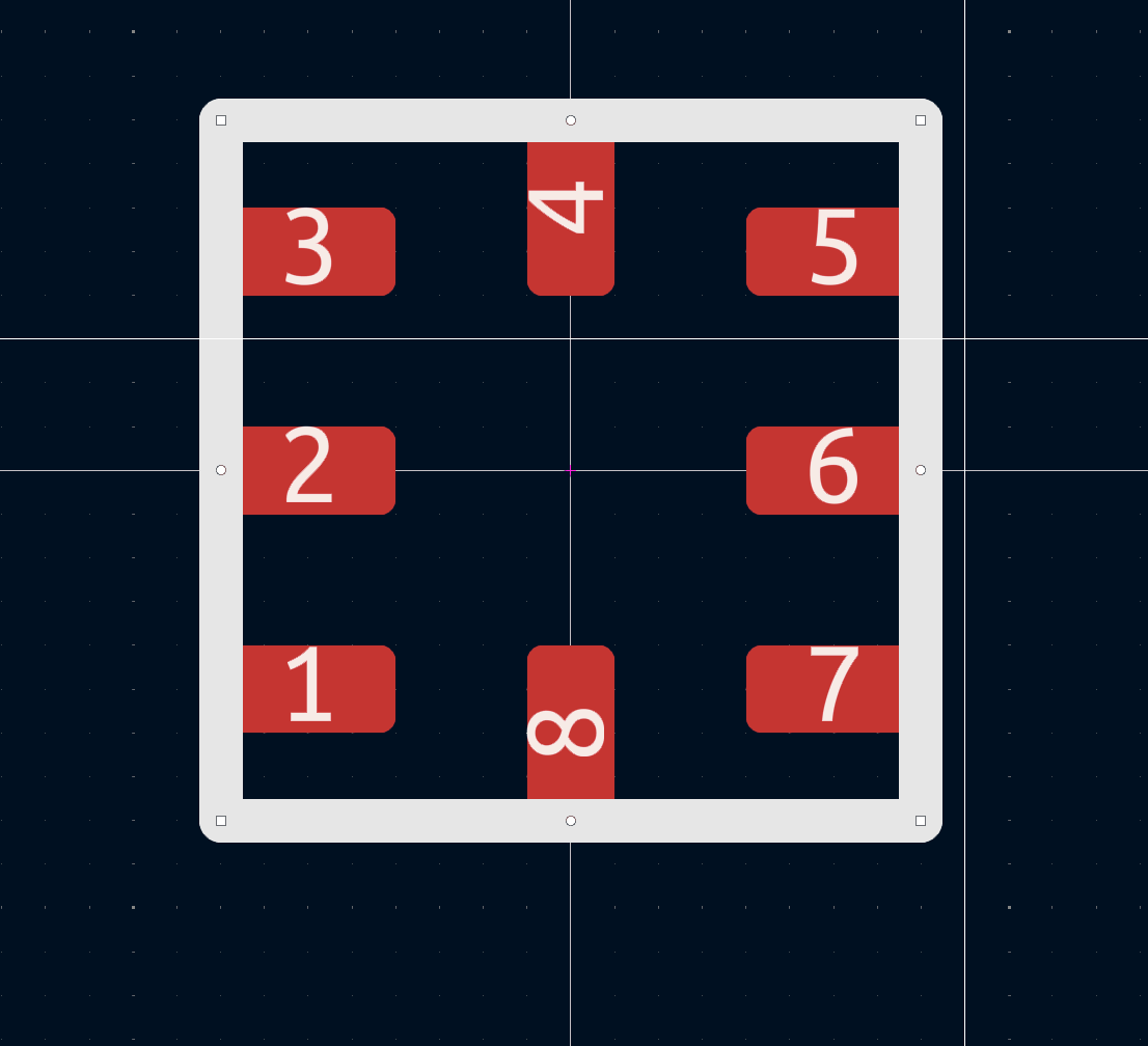
Then a Courtyard around the part:
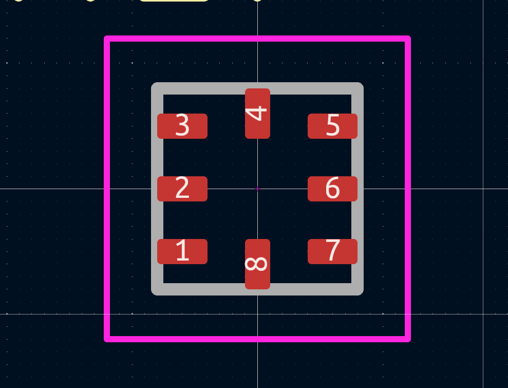
Followed by a Pin 1 indication
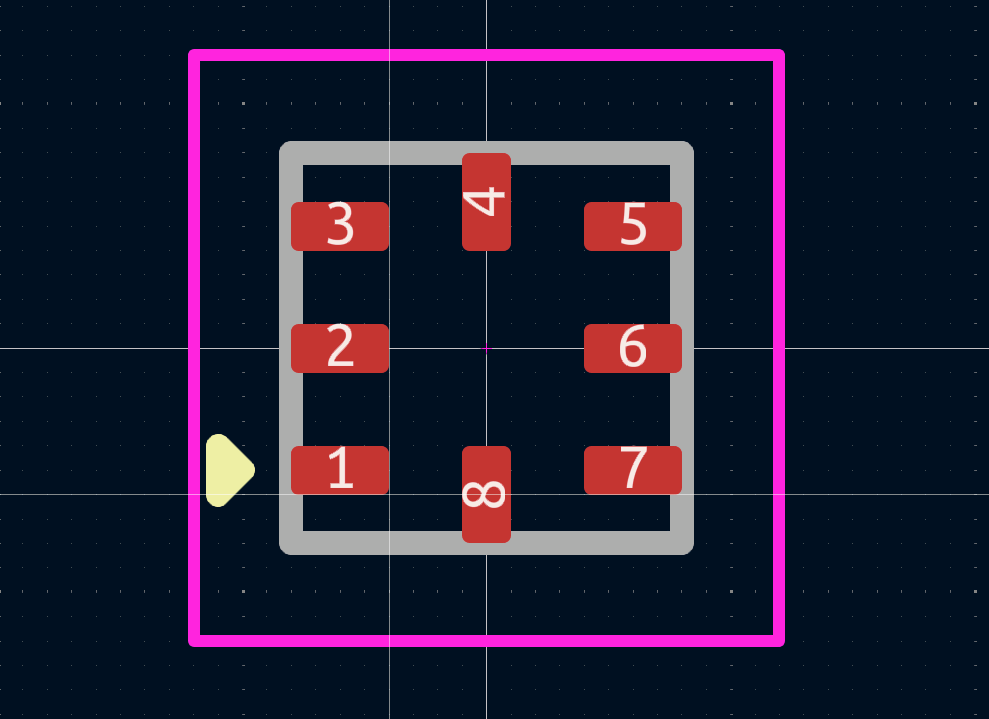
Last thing is to modify the footprint properties:
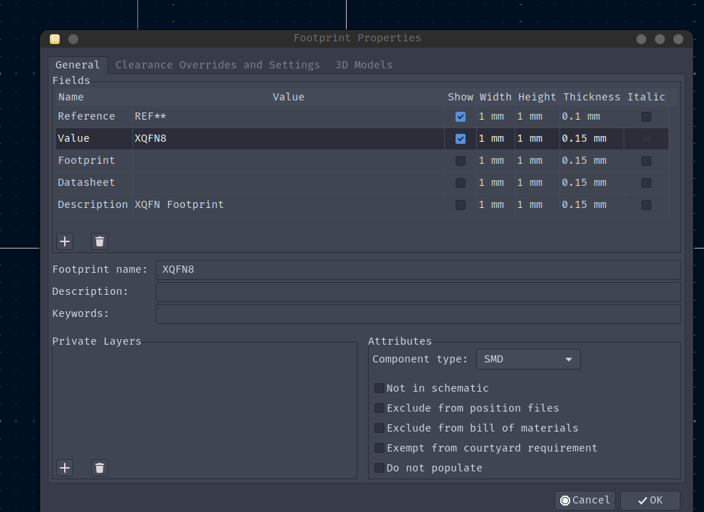
We can save and then use this footprint in the next project.
