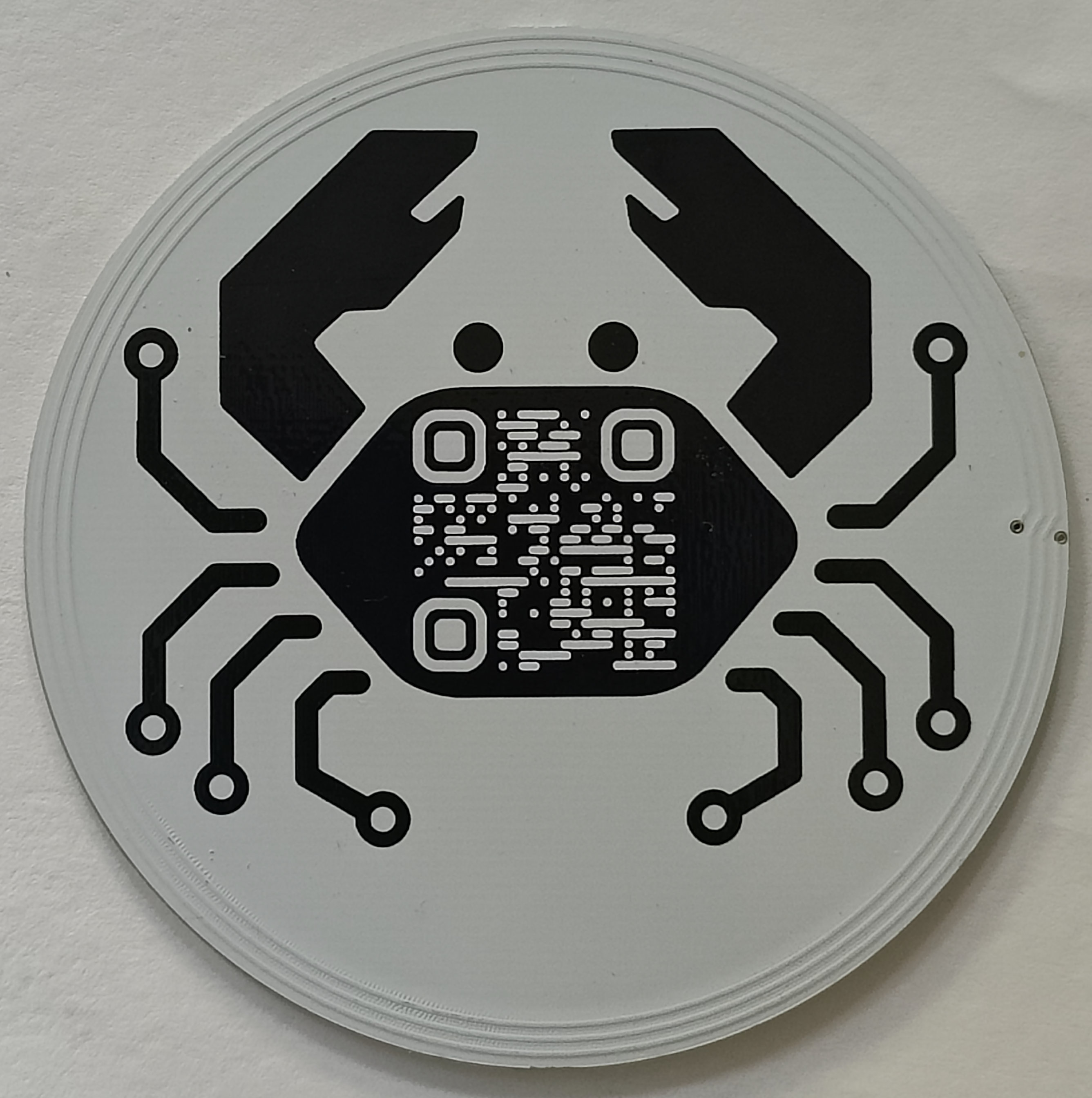
An NFC PCB business card can be a fun and unique way to promote yourself or your business.
Crab Labs designed and built these NFC PCB Business cards, the source files are here

I will show you how to design and build one using KiCad and JLCPCB
Prerequisites
- Understanding of basic circuit theory and electronics (video here)
- Working knowledge of KiCad (Tutorial here)
Primer on NFC (Near Field Communication)
Near Field Communication is a standardized series of protocols which define communication between two devices utilizing a 13.56 MHz carrier frequency (reference).
NFC devices need to be within several centimeters to communicate with each other.
Common NFC protocols are ISO 14443 (Most Common) and ISO 15693 (Newer, faster, more range). Most devices, including smartphones, natively support ISO 14443 communication; support for ISO15693 is not as widespread.
There are two main classes of NFC devices, Tags and Readers. This business card will be a tag and a smartphone or other device will be a reader.
NFC Tags store information that is procedurally read by a reader device when it gets close enough to be powered by it. The format and type of data that is read and interpreted is standardized but may or may not be supported based on the reader.
Preliminary Design
The first step in the design is deciding the big picture details of the design such the general shape of the card and what it will contain.
NFC Tags can have a large amount of data stored on then, some reader devices have less compatibility than others in regards to acting on the data in the tag. For example, contact cards (vCards) can be stored on NFC Tags but Apple IPhones are not able to automatically import or read them in to your contacts while most Android devices have native support.
The most universal data form is a simple url, it is recommended to store either a URL or phone number. If you or your company has a website or landing page that would be ideal.
As for the size and shape of the card there are very few limitations, the main limitation is in regards to the antenna. There should be an unbroken area of at least 2cm x 2cm which is dedicated for the NFC antenna, the larger the antenna is, the greater the range. You can and should create an interesting outline using tools such as Adobe Illustrator, Inkscape, or other Vector Graphics or CAD tools. Crab Labs recommends having no dimension greater than 3.5 inches (90 mm) in the x or y direction (a standard business card is 3.5" x 2" (90 x 50mm))
Crab Labs designed our version as a circle in order to use them as coasters or decor as well as to stand out.
Creating the Schematic
The following circuit is what was designed and used by Crab Labs
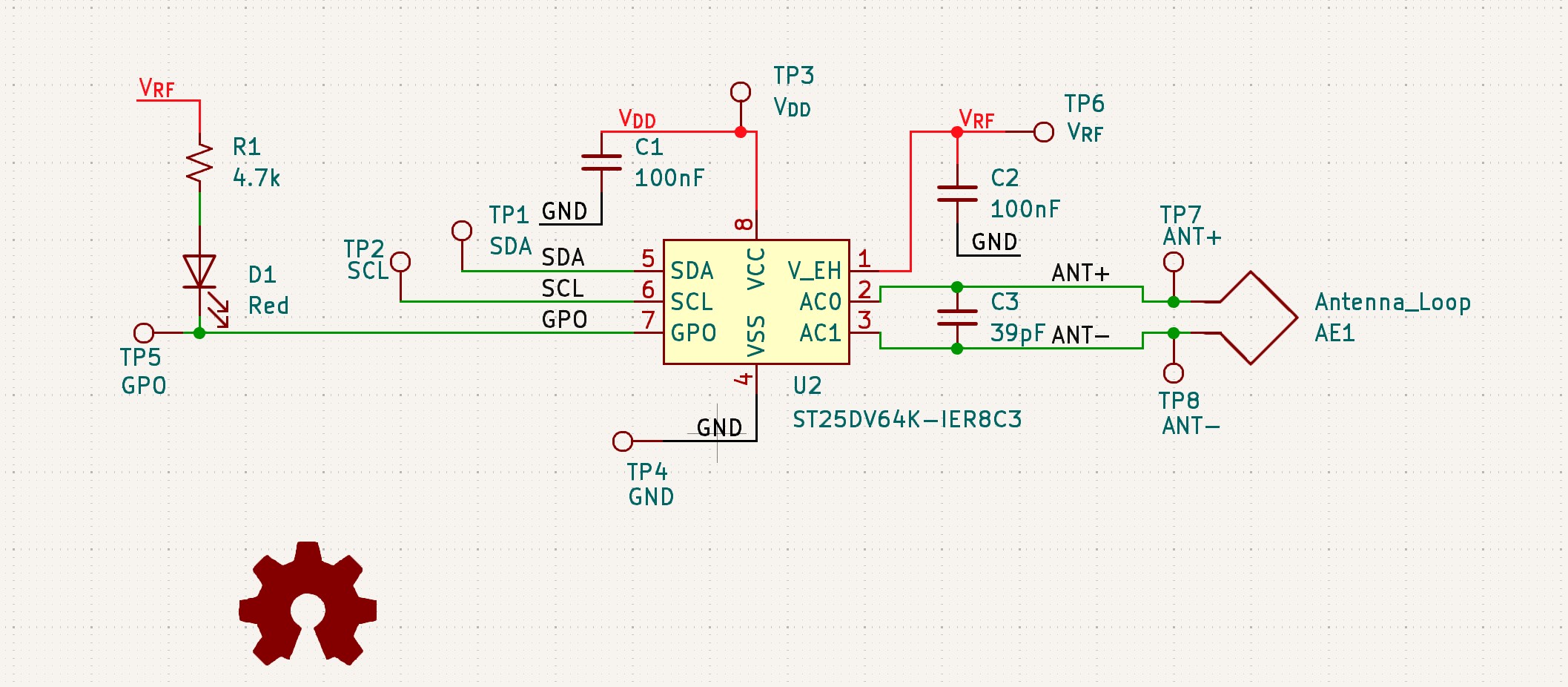
The circuit is relatively simple, it revolves around a NFC IC which handles all of the NFC communication.
More circuitry can be added as desired.
For a detailed breakdown of the schematic see the docs portion of the source repository located here.
Open KiCad and create a new project using Command+N or Ctrl+N
Find a location to create the project and name it something appropriate, such as “BusinessCard”
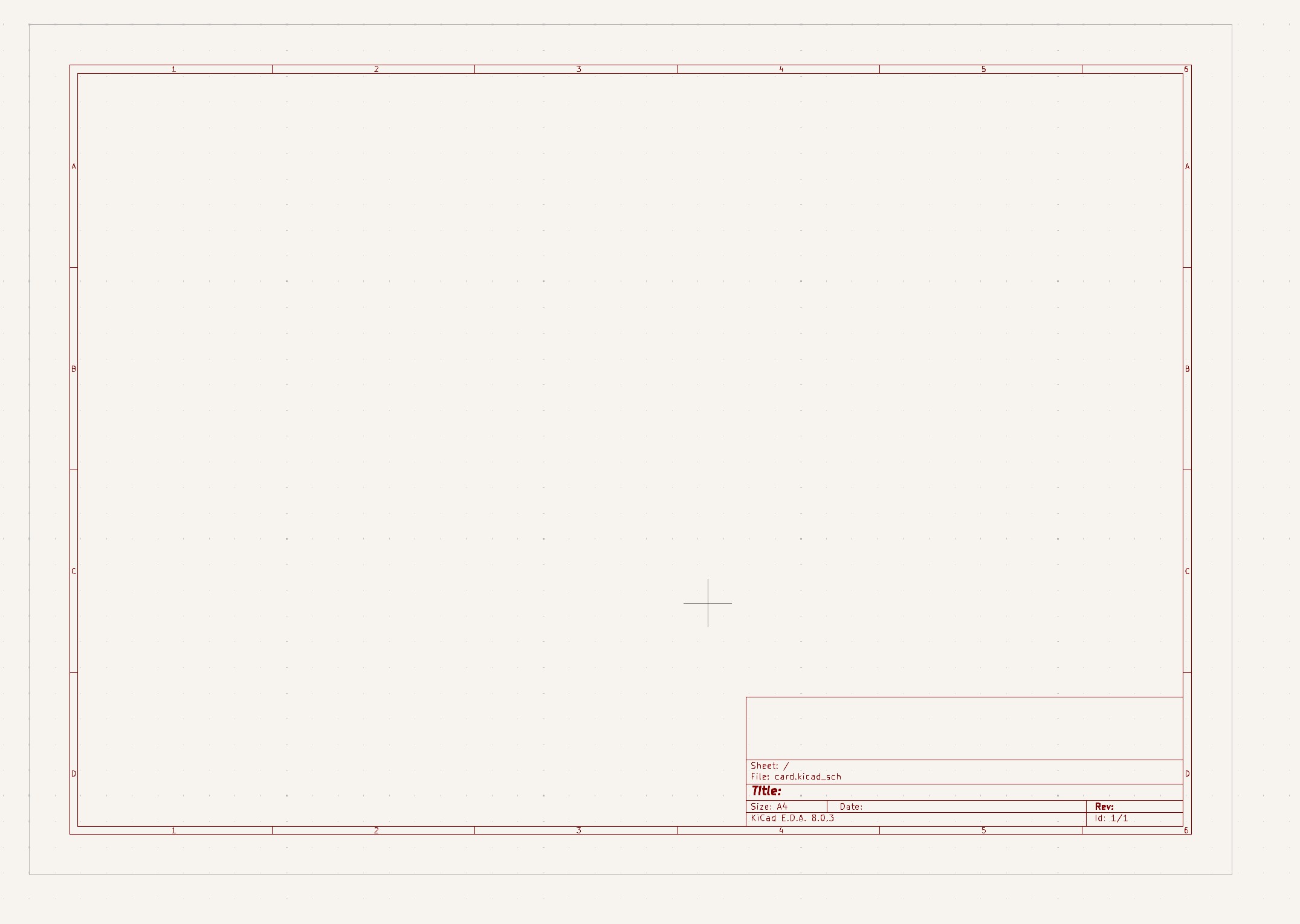
Once the project has been created, navigate to and open the schematic (the file called *.kicad_sch), it will look like this:
Selecting an NFC Tag IC
The most crucial decision in designing an NFC business card if the choice of NFC transponder or tag IC. It is generally recommended to chose a ISO 14443 chip as it is the most compatible.
There are a number of popular ISO 14443 NFC Tag ICs, such as:
Some of the most popular ISO 15693 NFC Tag ICs are:
- ST25DVx by ST Microelectronics (x = 04K, 16K, 64K)
- M24LRx by ST Microelectronics (x = 04, 16, 64)
- N24RFx by onsemi (x = 04, 16, 64)
The most important factor in finding the right transponder chip is the memory size, you generally want as much memory as you can afford.
Note: Crab Labs recommends using the M24S or ST25DV series of transponders, they are plentiful, affordable, and easy to work with.
Sourcing NFC Tag ICs
If you are comfortable hand soldering components you can look for components from any source (Octopart searches multiple sources around the web at once). Chose tags with SO-8 or similar packages if you plan to hand assemble unless you have access to advanced tools or have significant experience.
If you can’t or don’t want to hand assemble PCBAs, then it is recommended to look for components on LCSC. If the component is available on LCSC then your design can be fully built and assembled at JLCPCB in a timely manner. If you do not chose a component that is available on LCSC you will either have to hand assemble that component or have the part be ordered on the side (this is more expensive, takes longer, and is more difficult).
Open KiCad and create a new project using Command+N or Ctrl+N
Find a location to create the project and name it something appropriate, such as “BusinessCard”
Once the project has been created, navigate to and open the schematic (the file called *.kicad_sch), it will look like this:
Placing the Components
Press “A” to add a symbol, this menu will appear. If you chose the ST25DV, then the component will be available, else you will need to add the component library to use it (see here for tutorial)
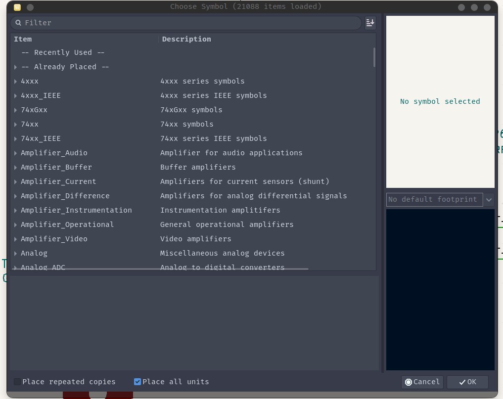
Search for the component you want to add:
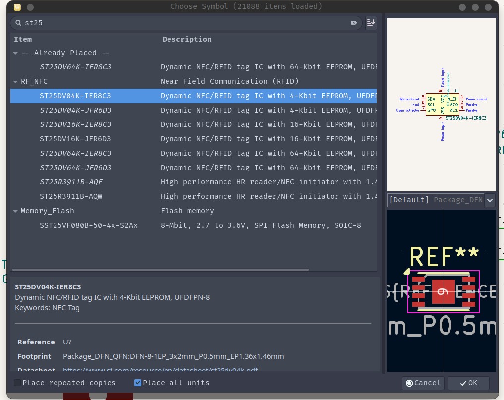
Make sure that you play close attention to the full name and that the symbol and footprint line up with that is on the datasheet of the part that you selected. Double click the item and click somewhere to place it, preferably in the middle of the schematic.
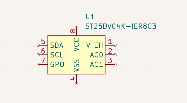
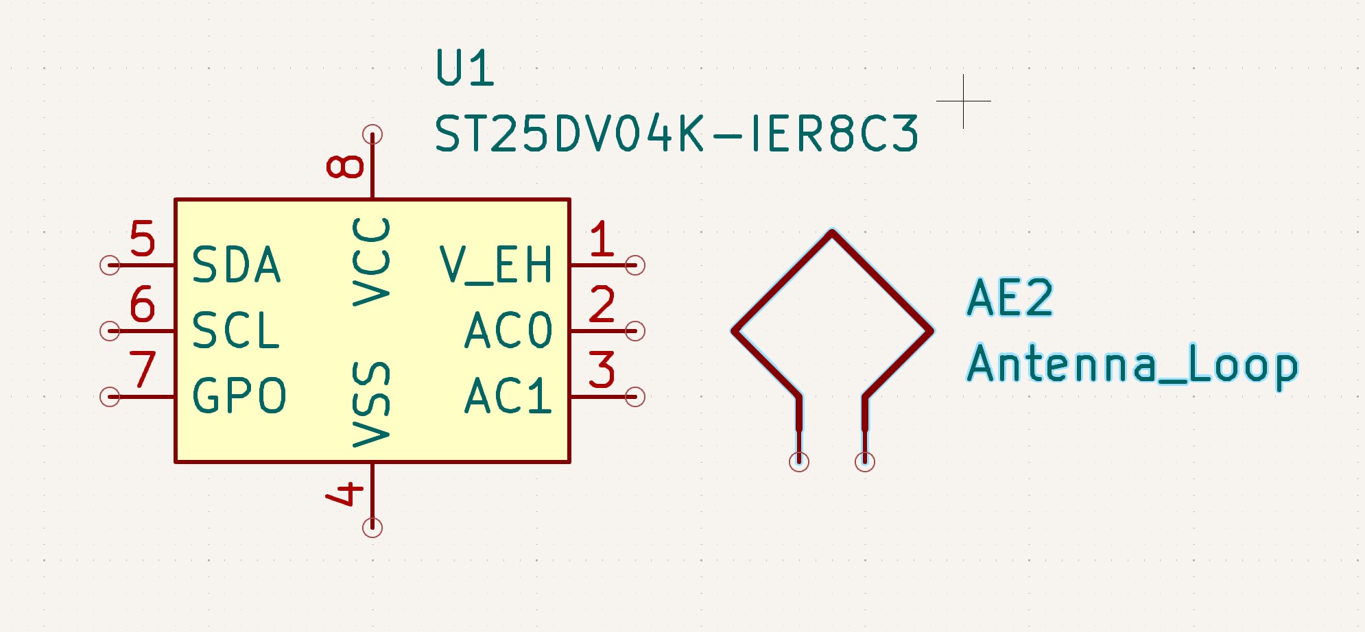
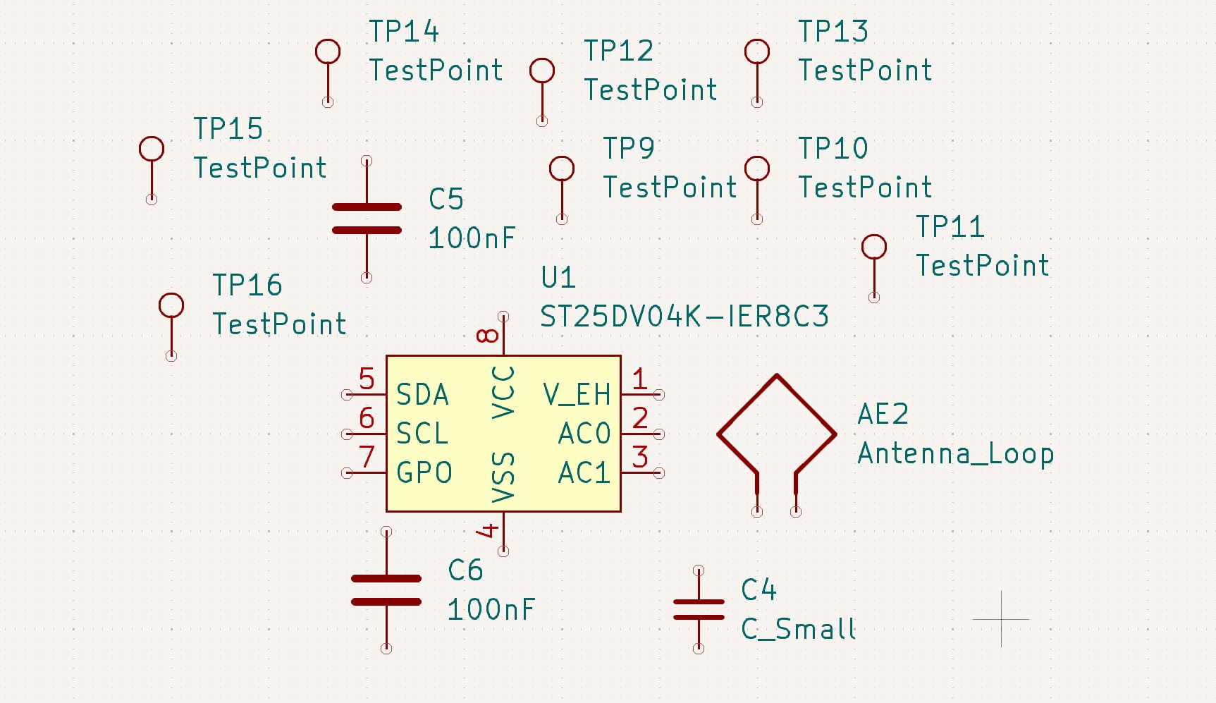
Next is to add any supporting circuitry, namely the antenna and storage capacitors.
Add a loop antenna symbol by pressing “A” and searching for “Antenna_Loop”.
Add a tuning capacitor by pressing “A” and searching for “C_Small”. The value of this capacitor is determined by the shape and properties of the antenna. It’s value will be set when the antenna is designed.
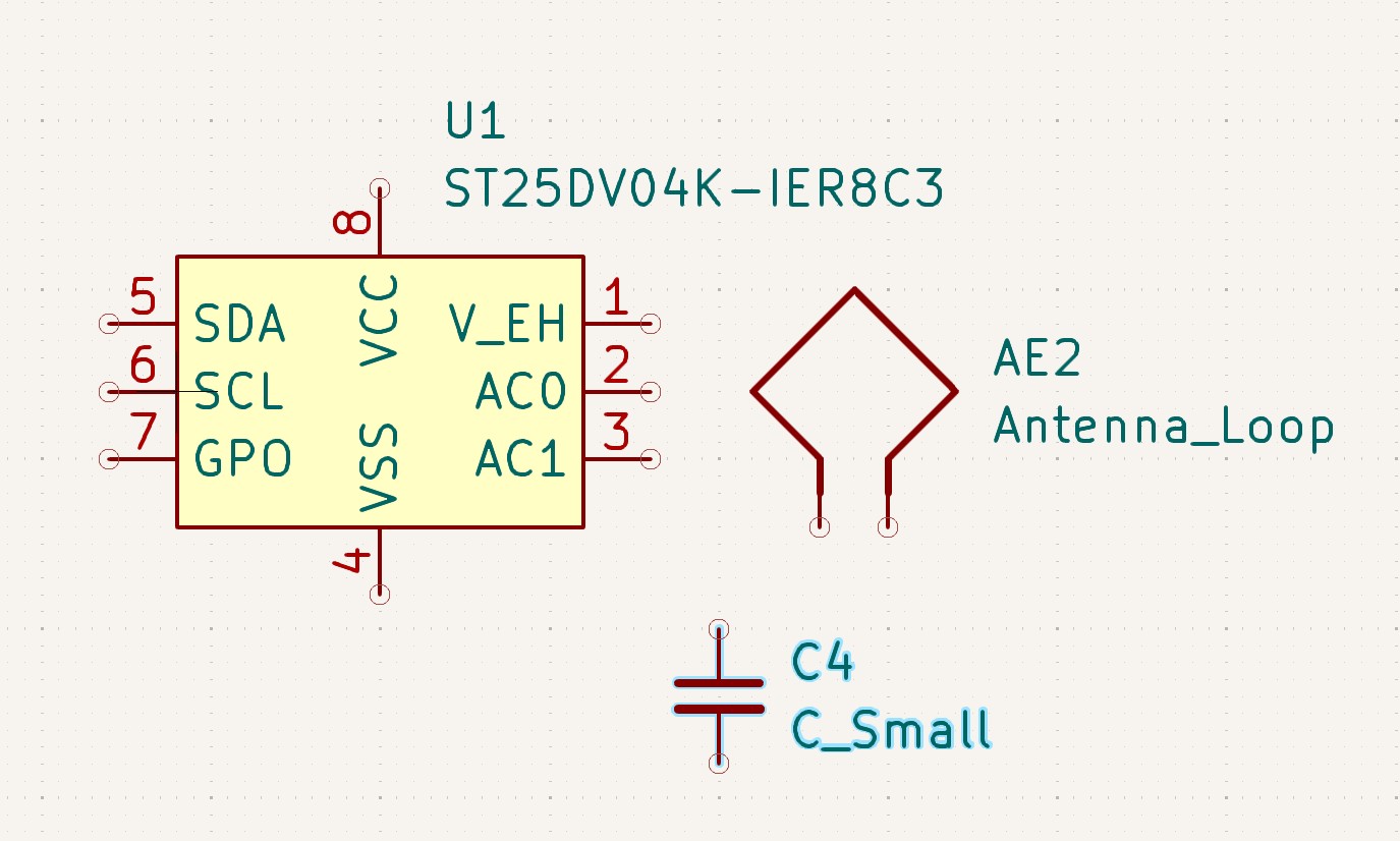
These three components are technically all that is required to make this device work as intended. If you don’t care about adding additional niceties such as test points or status LEDs then proceed to here
If the device contains an external voltage supply pin (i.e. VDD or VCC), then a capacitor should be added. This capacitor should have a value of 100nF or more. Press “A” and look for “C”. Once placed, click on it and press “E” in the “Value” field enter “100nF”.
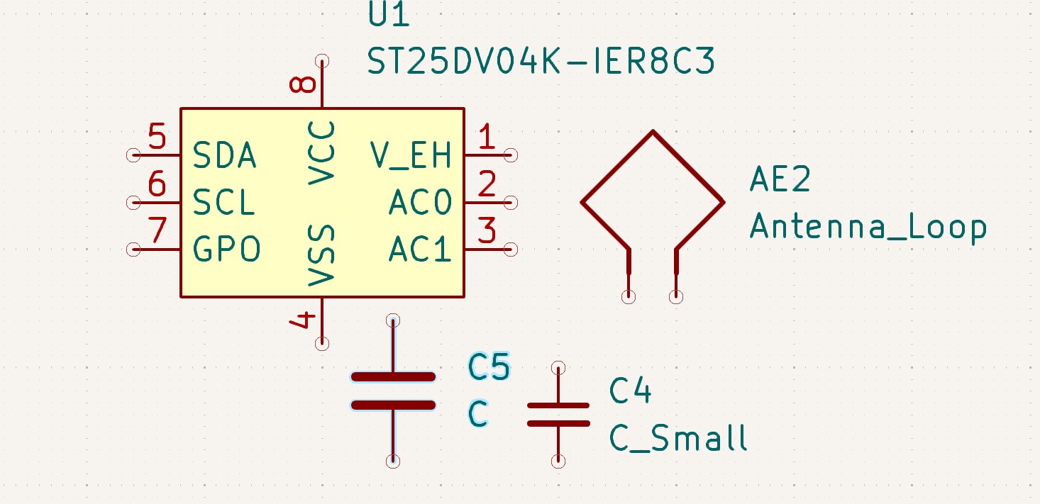
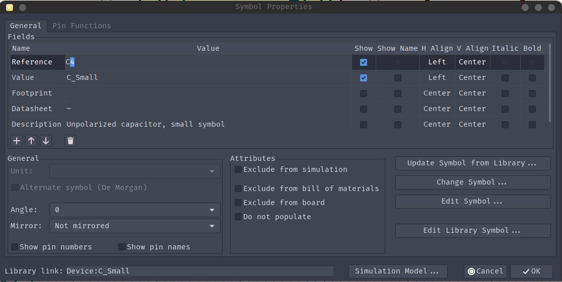
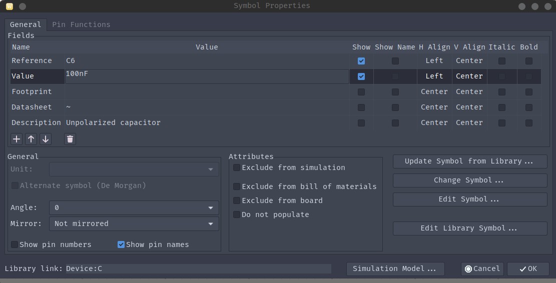
If the device has energy harvesting capabilities, then a capacitor should be added for the energy harvesting voltage (search the data sheet for this information). Press “A” and look for “C”. A recommended capacitance by Crab Labs is 100nF, if the datasheet suggests a different value, use that value instead
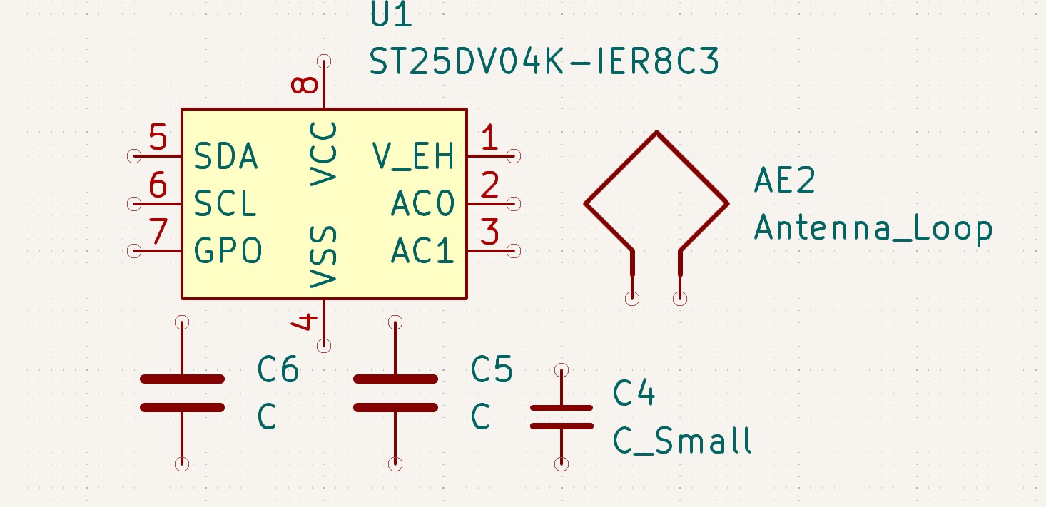
It is recommended to add test points to all of the pins in order to properly test and debug the functionality of the device. This is entirely optional but highly recommended in the first revision of a design. Press “A” and search for “TestPoint”, it is recommended to use the “TestPoint” symbol but “TestPoint_Small” works just as well.
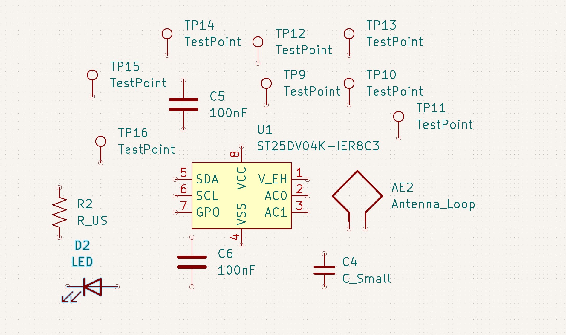
If you would like a status LED and the tag that you chose supports it (has energy harvesting and an output pin) then a resistor and LED will be needed. Press “A” and search for “R_US” (“R” if in the E.U.) as well as “LED” and place one of each.
Wiring Components
The next step is to properly connect the components so that the circuit is valid
Before wiring can be completed the components should be moved as close to where they should be connected (e.g. the antenna tuning capacitor should be placed next to the antenna pins)
An example of this would look like this:
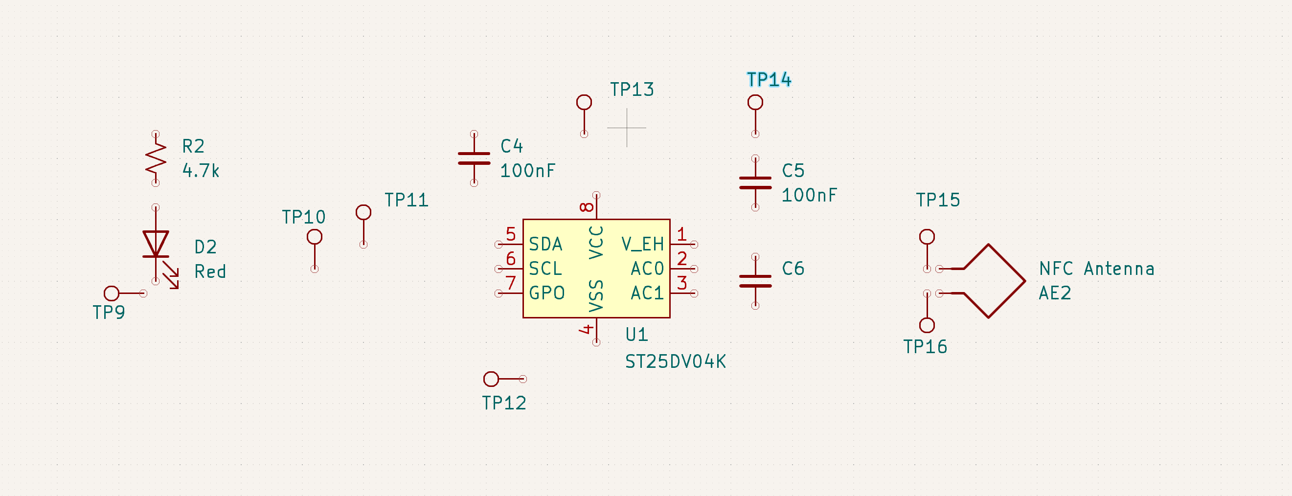
We see that the test points are near the pads which they will be connected to and the capacitor for V_EH and VCC are close to the pins. The antenna and tuning capacitor are in line with the pins which they should connect to (as per the datasheet).
To begin wiring the components together, press “W” to begin placing wires, clicking on the pin connection point will also start wiring.
Start by wiring the antenna to the tuning capacitor to the pins on the Tag IC, make sure to include the test points if your design has them:
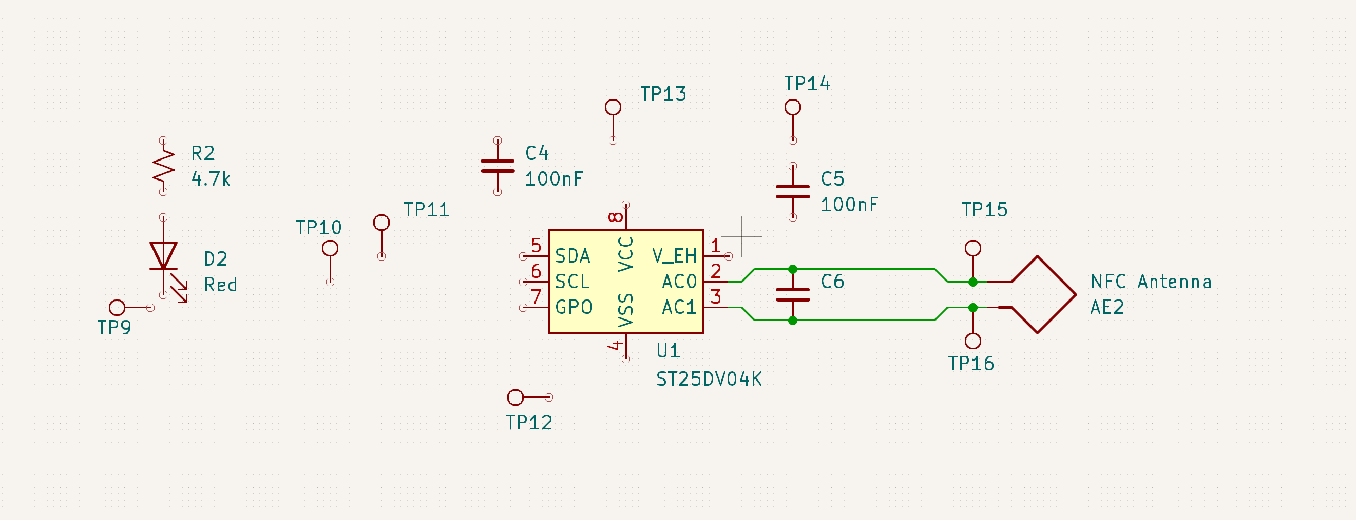
Your wires don’t need to be in the same style as shown here, as long as they are connected you are good.
Now connect the rest of the components in the same style, if you have to cross over another wire to complete a connection then leave it unconnected for now.
Labeling Nets and Finishing Connections
An important step in any PCB project is defining the net names, this allows for significantly better readability as well design clarity.
In order to label a wire, press “L” in the schematic editor
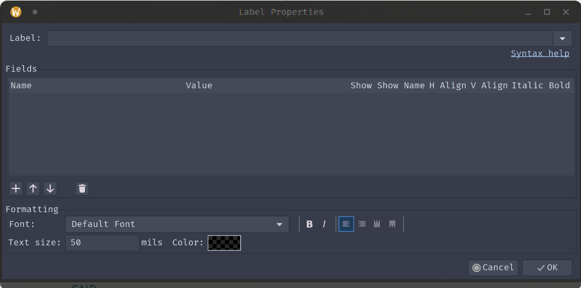
Place this label on the wire that you want to define the name for.
If you have a pin that needs to be connected and couldn’t be connected cleanly before, then you can draw a small segment of wire where the pin is and where it needs to connect. If you put a label on both of the wire segments, then they will be recognized by KiCad as connected.
An example of a labelled and connected schematic can be seen below
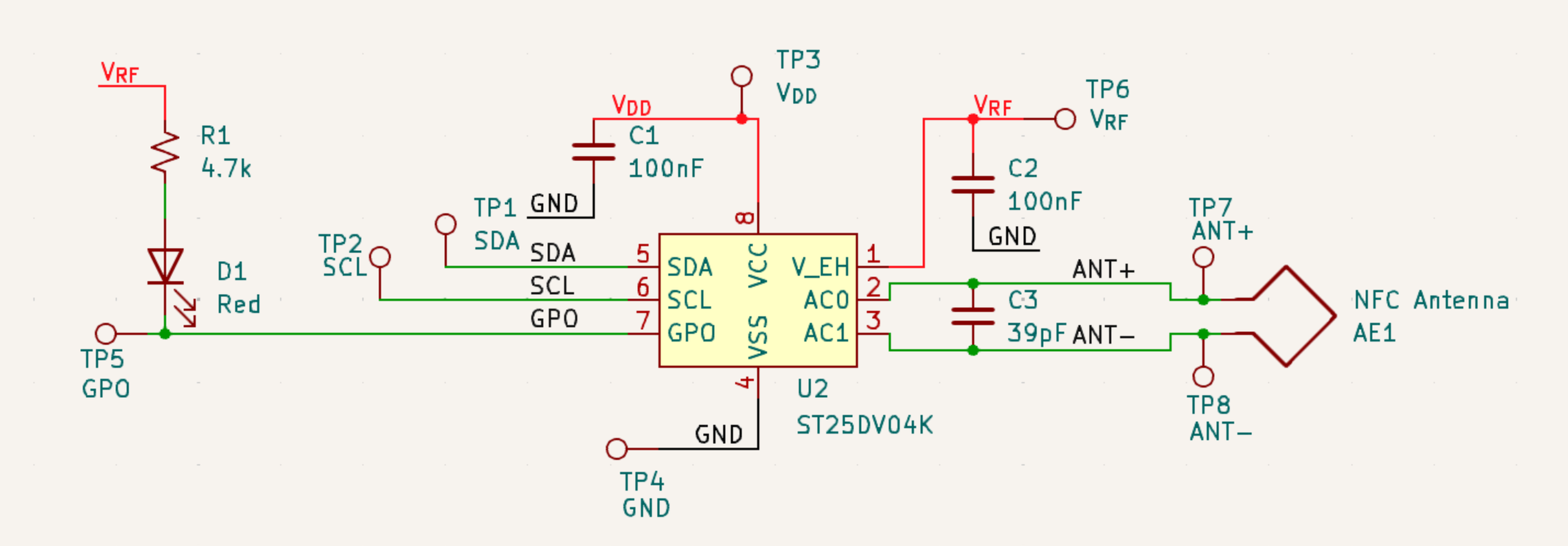
If there are any connections or pins that you do not want to connect, add a “No Connect” flag using “Q”
Checking the Schematic
Before the schematic can be turned in to a PCB, the schematic must be verified to ensure that proper connections are made and circuit is valid.
To validate the schematic, navigate to Inspect -> Electrical Rules Checker. Once in the menu press “Run ERC”
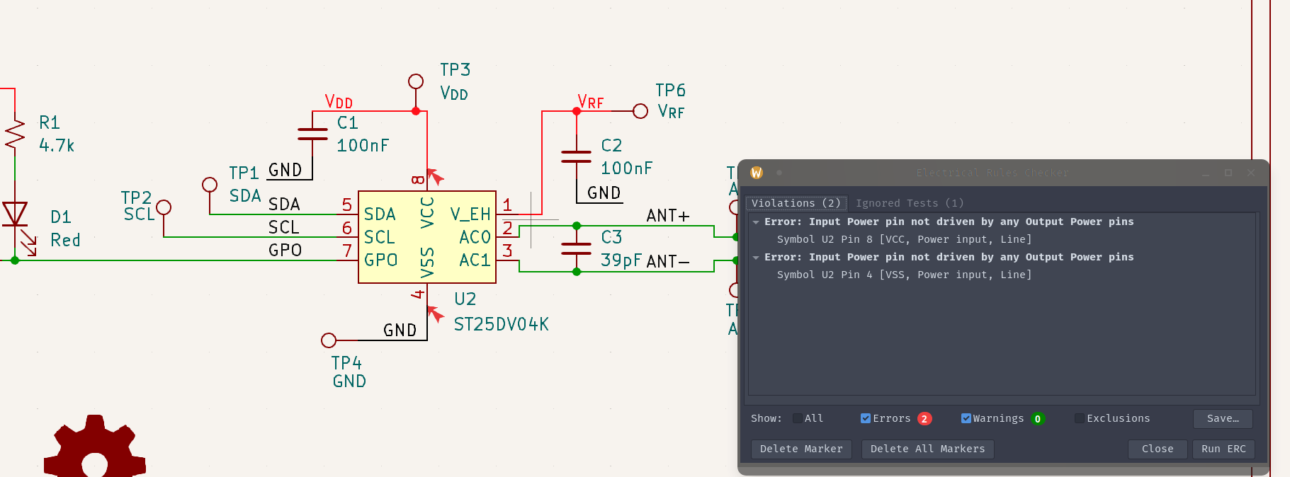
The most common error will likely be “Power pin not driven”. In order to fix this, place a “PWR_FLAG” symbol on the net indicated. Any other issues should be addressed and the schematic should not generate any errors or warnings.
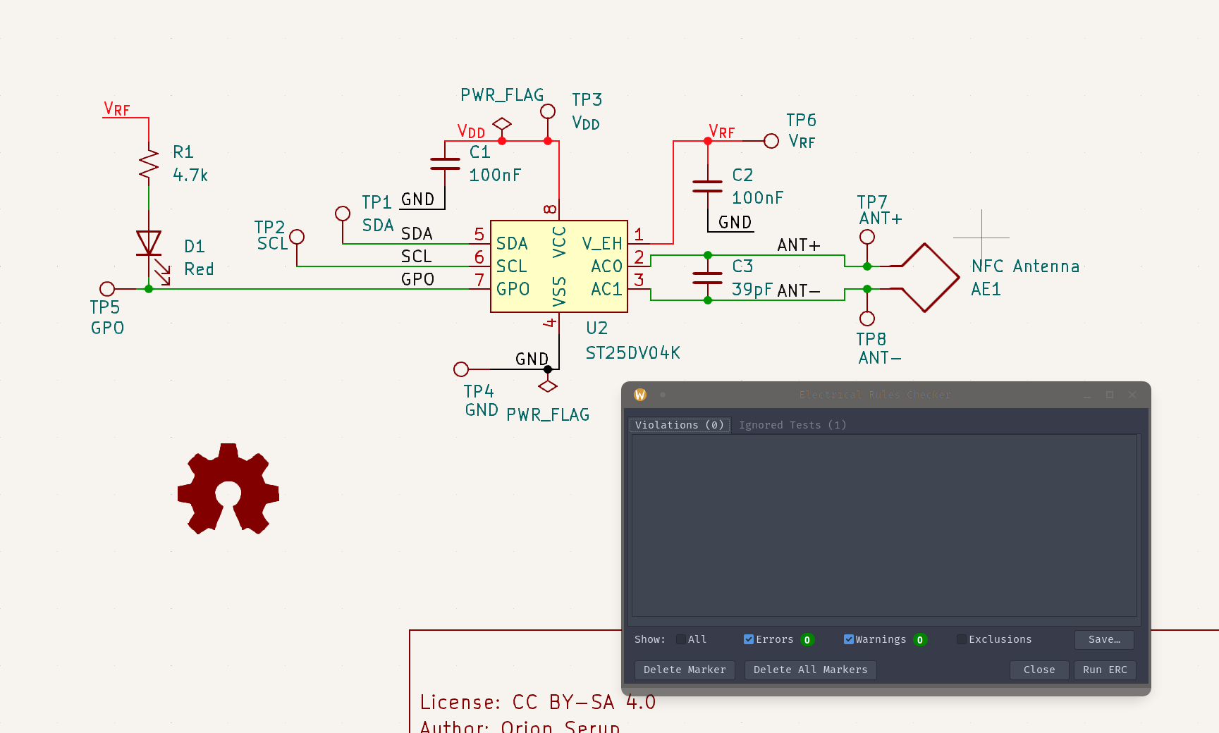
Now that the schematic is functionally complete and checked we should begin the transition to the actual PCB/Layout.
Assigning Component Footprints
Before the circuit can be exported to a PCB, the components need to be assigned a physical footprint (i.e. what the connections to the board look like).
In order to assign a footprint to a component click on it and press “E”, navigate to the “Footprint” field and click on the books icon:
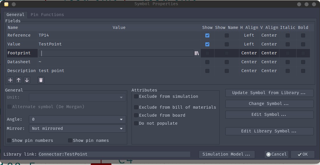
Then you will enter the footprint selection menu
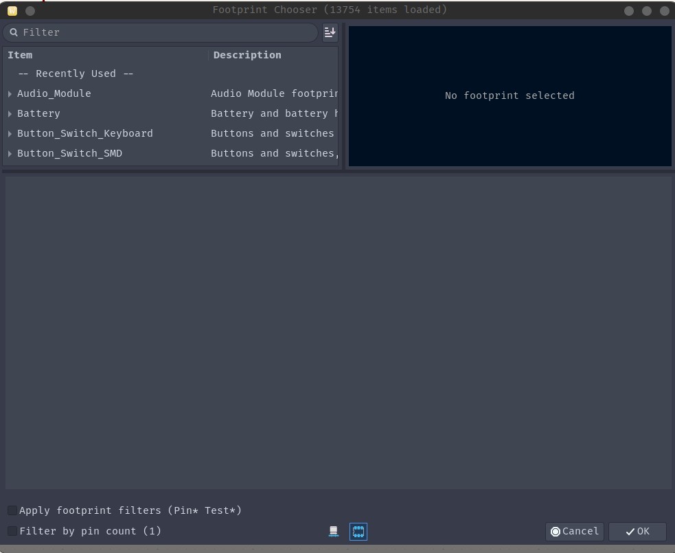
If you plan on hand soldering the components these footprints are recommended:
- Capacitors: C_0805_2012Metric (smaller) or C_1206_3216Metric
- Resistors: R_0805_2012Metric (smaller) or R_1206_3216Metric
- TestPoints: TestPoint_Pad_D2.0mm
- LEDs: LED_0805_2012Metric (smaller) or LED_1206_3216Metric
If you plan on having JLCPCB or another manufacturer assemble these boards then the following footprints are recommended:
- Capacitors: C_0201_0603Metric (smaller) or C_0402_1005Metric
- Resistors: R_0201_0603Metric (smaller) or R_0402_1005Metric
- TestPoints: TestPoint_Pad_D1.0mm
- LEDs: LED_0402_1005Metric
Assign all of the footprints as needed
The antenna will need it’s own custom footprint, which will be created later
Creating the Layout
Setting Up the PCB
Every design must have specific design rules set. These design rules define different properties of the physical design such as spacing and hole sizes. These rules ensure that your design can be made by your manufacturer. Generally these rules will come directly from the manufacturer, but for this project very safe design rules will be provided to ensure that the design can be manufactured at almost any manufacturer.
To set the design rules first select the “mil” icon on the left side bar (sets the dimensions to mils) and navigate to “File -> Board Setup”. Once in the Board Setup menu, navigate to the “Design Rules” tab and click in to the “Constraints” item.
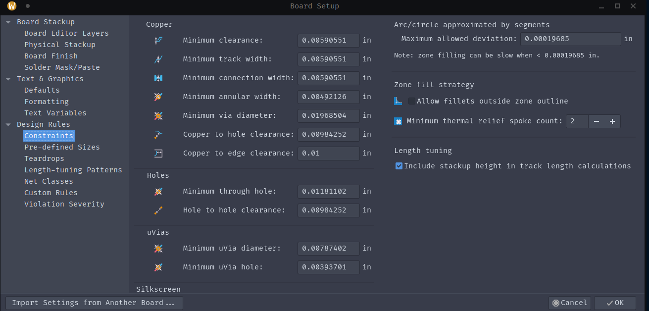
The following constraints will be used for this design:
- Minimum Clearance: 6 mils (.15mm)
- Minimum Track Width: 6 mils (.15mm)
- Minimum Connection Width: 6 mils (.15mm)
- Minimum Annular Width: 4 mils (.1mm)
- Minimum Via Diameter: 20 mils (.5mm)
- Copper to Hole Clearance: 10 mils (.25mm)
- Copper to Edge Clearance: 10 mils (.25mm)
- Minimum Through Hole: 12 mils (.3mm)
- Hole to Hole Clearance: 10 mils (.25mm)
These are very safe rules for a 2 layer 1oz/ft^2 PCB which is the cheapest and fastest to produce PCB available.
We then need to set the sizes of traces/tracks and vias, this can be done in the “Pre-Defined Sizes” menu
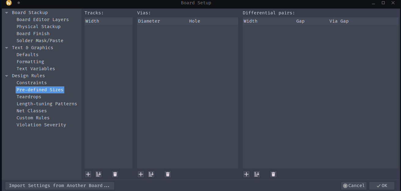
We want to add a number of different track and via sizes, they can be added by pressing the plus on the bottom of the menu.
We will add the following tracks:
- 6 mils
- 8 mils
- 10 mils
We will add the following vias:
- 12 mil hole 20 mil diameter
Now we can begin designing the PCB, if you would like to further customize the PCB feel free.
Importing Parts from the Schematic
The first step in creating the layout is navigating to the PCB editor. This can be done by navigating to Tools -> Switch to PCB Editor. Once in the PCB editor you want to import the schematic components by navigating to Tools -> Update PCB from Schematic.
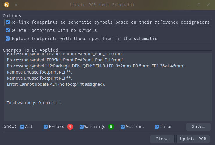
Click “Update PCB”, you will likely have one error for the antenna footprint. If there are any more errors you will need to go back to the schematic and fix the errors.
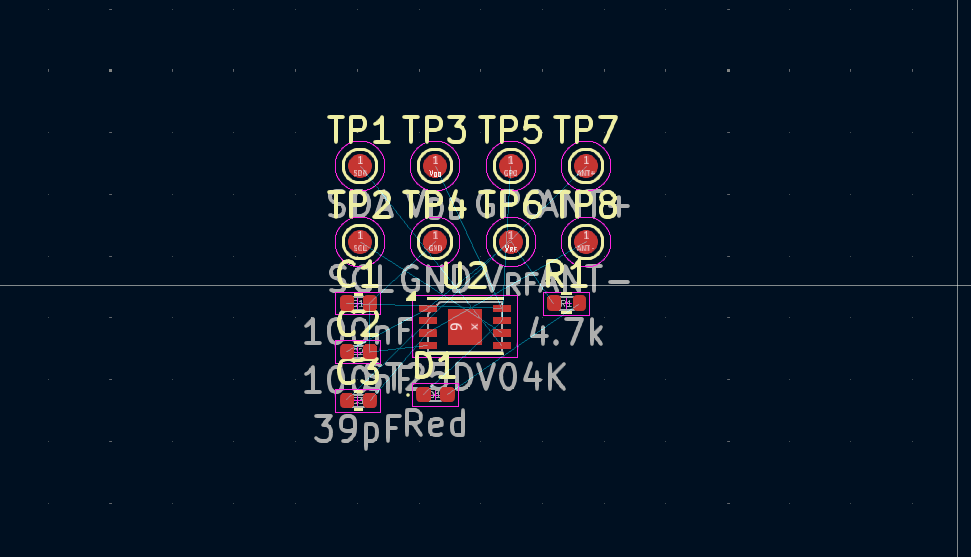
The next step is to create the outline of the board
Creating the Board Outline
Importing an External Outline
If you have created a desired outline using outside CAD or graphics tools, they can be directly imported in to KiCad. Navigate to File -> Import -> Graphics.
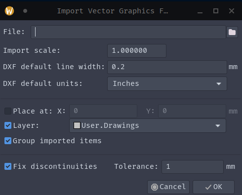
This tool allows you to import SVG or DWG/DXF files to any layer of the PCB. Select the proper scaling and units if using DWG/DXF. The layer to import to is “Edge.Cuts”.
Crab Labs recommends using the measure tool on the imported graphics to ensure they are properly sized according to what you drew, if they are not correctly sized, they may need to be deleted and reimported with a different scale.
Once the outline is properly imported, check that is continuous. See the next section for details.
Creating Outline in KiCad
If you plan to create your own board outline in KiCad you can use, the line, or any of the polygon tools.
We will be creating a simple rectangular card with standard business card dimensions of 3.5" x 2" (90 x 50mm) for demonstration. Using the “Draw Rectangle” tool in the toolbar when the “Edge.Cuts” layer is selected we will draw a rectangle with the dimensions indicated. It is recommended to set your grid to the greatest possible value which is cleanly divisible by the height and width
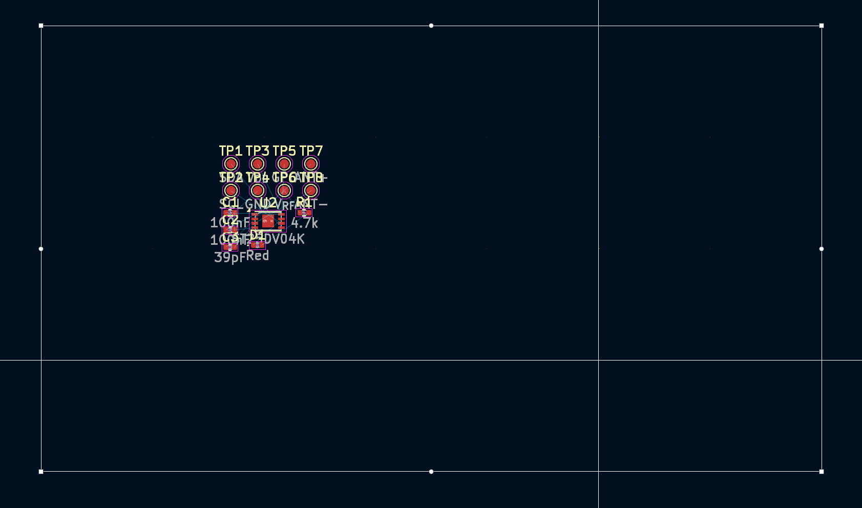
Once the outline is completed it is recommended to check the continuity of the outline, especially if the outline contains many parts or is imported . The easiest way to check this is to use the 3-D Viewer, this can be accessed through “View -> 3D Viewer”
A clean outline will have no errors or indications, like this (colors may not be the same):

If the outline is discontinuous or otherwise has issues it will look like this:
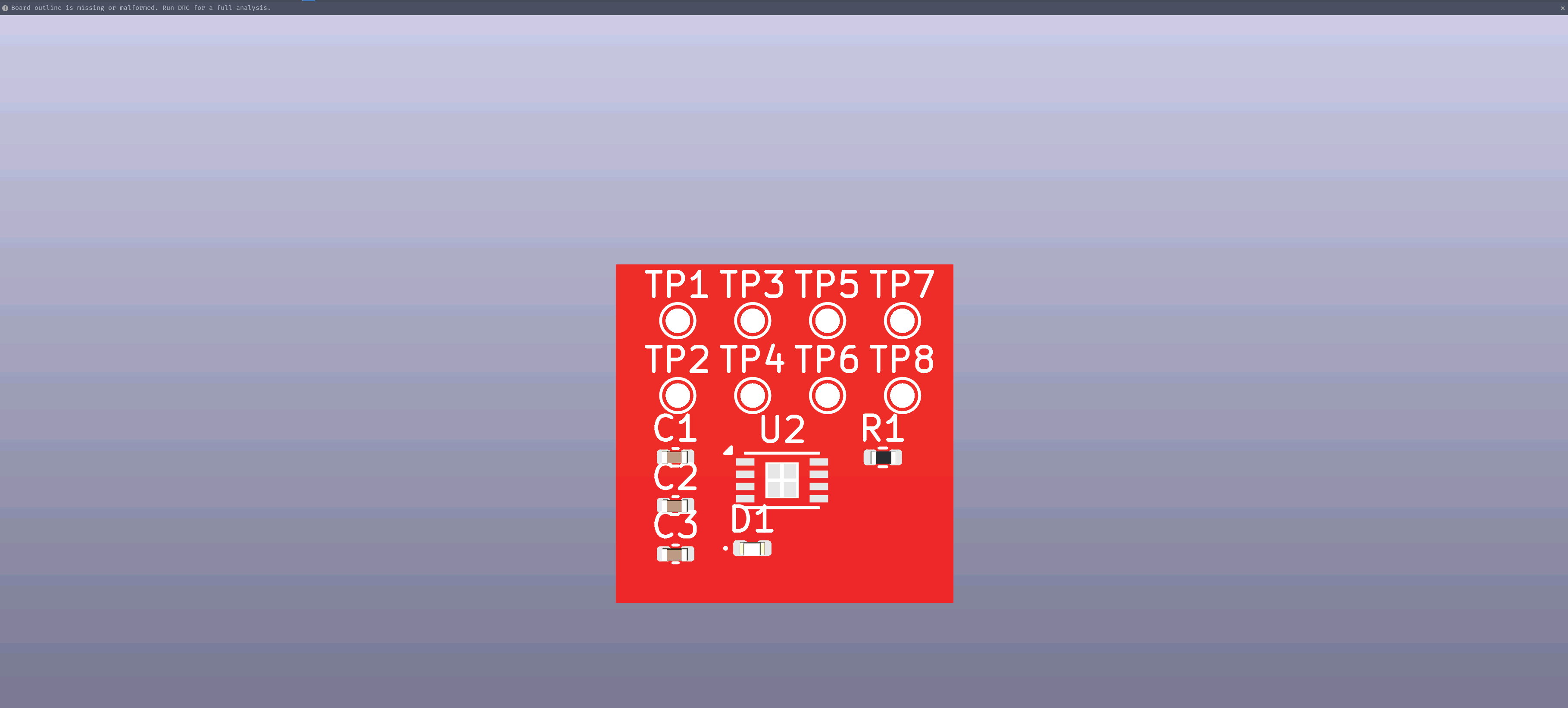
There will be a warning on the top of the screen, to diagnose where the issue lies with the best accuracy, a DRC check will need to be done. See Checking the Layout for more information
Placing the Footprints
Now that the components and outline are placed, it is time to place them appropriately. This means we need to generate the antenna footprint so that all of the components can be accounted for. If you have already designed an antenna then skip to Connecting the Components.
Make sure to only place parts on one side. If there are parts on both sides the cost of manufacturing goes up substantially. This only applies to physical items such as resistors, items such as test points can be on either side of the PCB with no issue.
Designing Antenna Footprint
Antenna construction and geometry is very crucial in the performance of the NFC business card. It is recommended to calculate the antenna characteristics and geometry before implementing it as a footprint.
Calculating Antenna Characteristics
When creating an antenna there are three main geometries: Spiral, Rectangular, and Circular. The most common and easiest to create is rectangular. Crab Labs designed a spiral antenna but recommends a rectangular antenna.
ST has an online calculator for rectangular antenna characteristics here. ST has an application note explaining NFC antenna design here.
An additional rectangular antenna calculator is here
It is recommended to have an antenna inductance of 1-4 uH.
Your design will have the following constraints:
- Track/Trace width > .15 mm (6 mils)
- Track/Trace Gap > .15 mm (6 mils)
- Trace Thickness: 35 um (1 oz/ft^2)
- Substrate Thickness: 1.6mm (61 mils)
- Substrate Relative Permittivity: 4.6
Referring to the preliminary design of the card manipulate the parameters of the design so that you get the desired inductance value within the area that is dedicated for the antenna.
If you desire to create a custom shape other than rectangular, the formulas in the application note must be used to calculate the inductance.
Designing the Footprint
In order to create a custom footprint a custom footprint library must be created. See this tutorial for guidance regarding the creation of libraries.
In order to create an antenna footprint it will require some different techniques than shown in the mentioned tutorial. Create a new footprint with an intuitive name such as “NFCAntenna”.
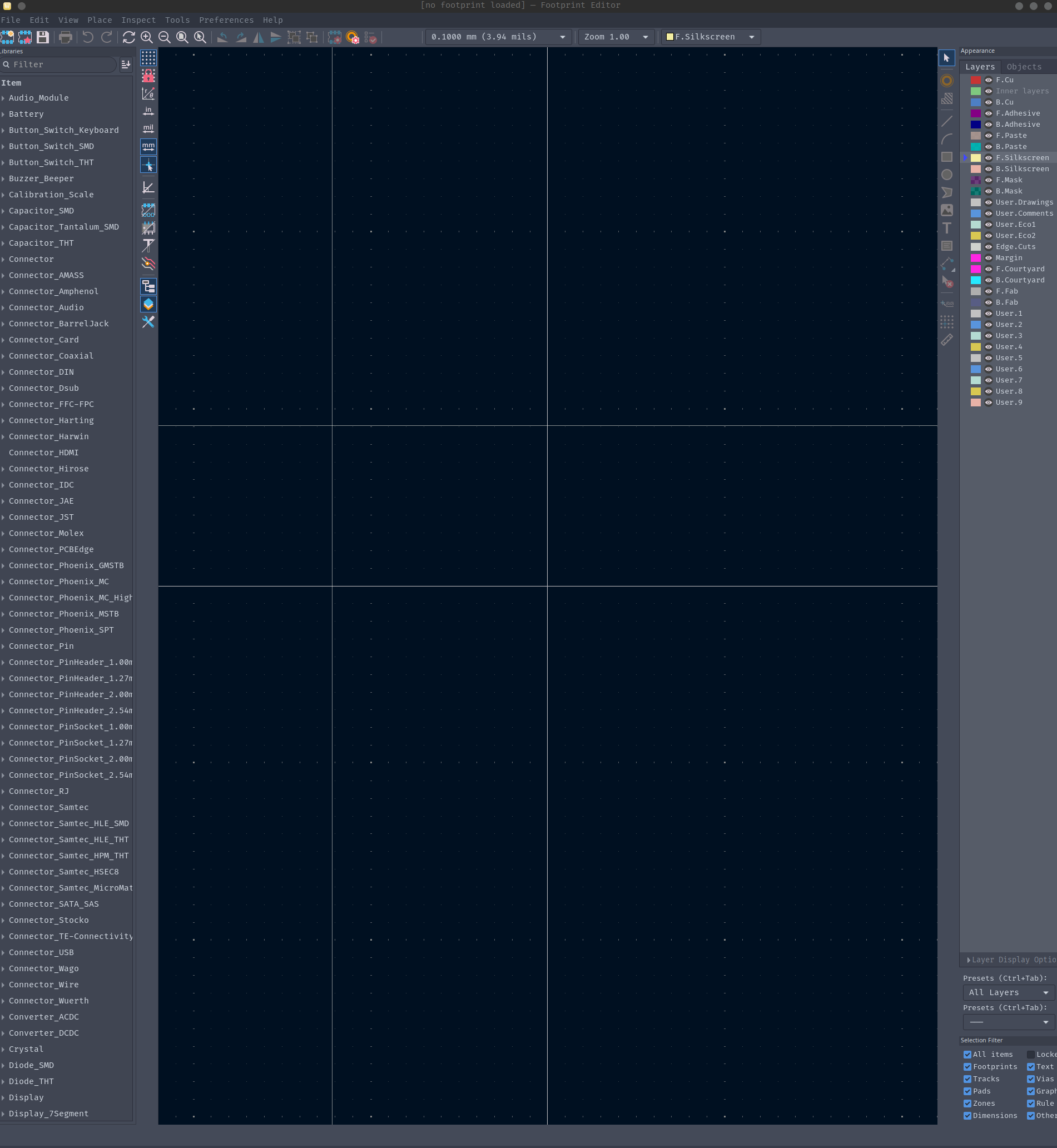
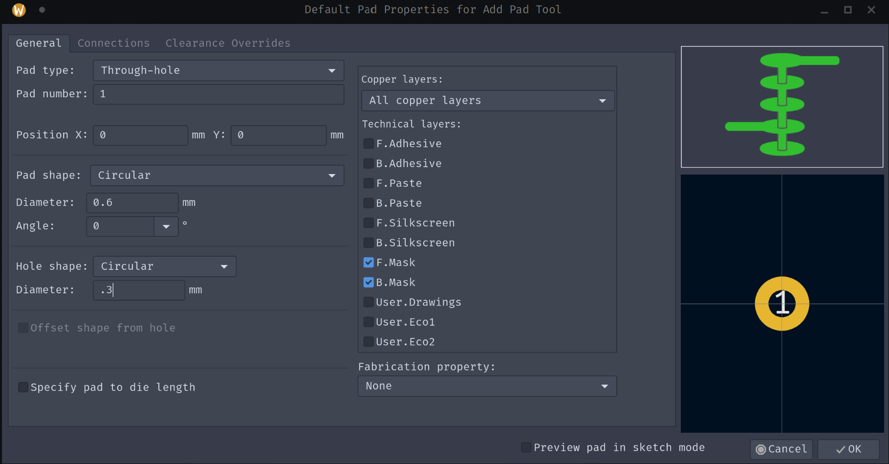
The first step is to create the pads that are used to connect to the rest of the circuit. Modify the pad properties and make the pad a through hole pad with a hole greater than .3 mm (12 mils) and an outer diameter greater than .5 mm (20 mils).
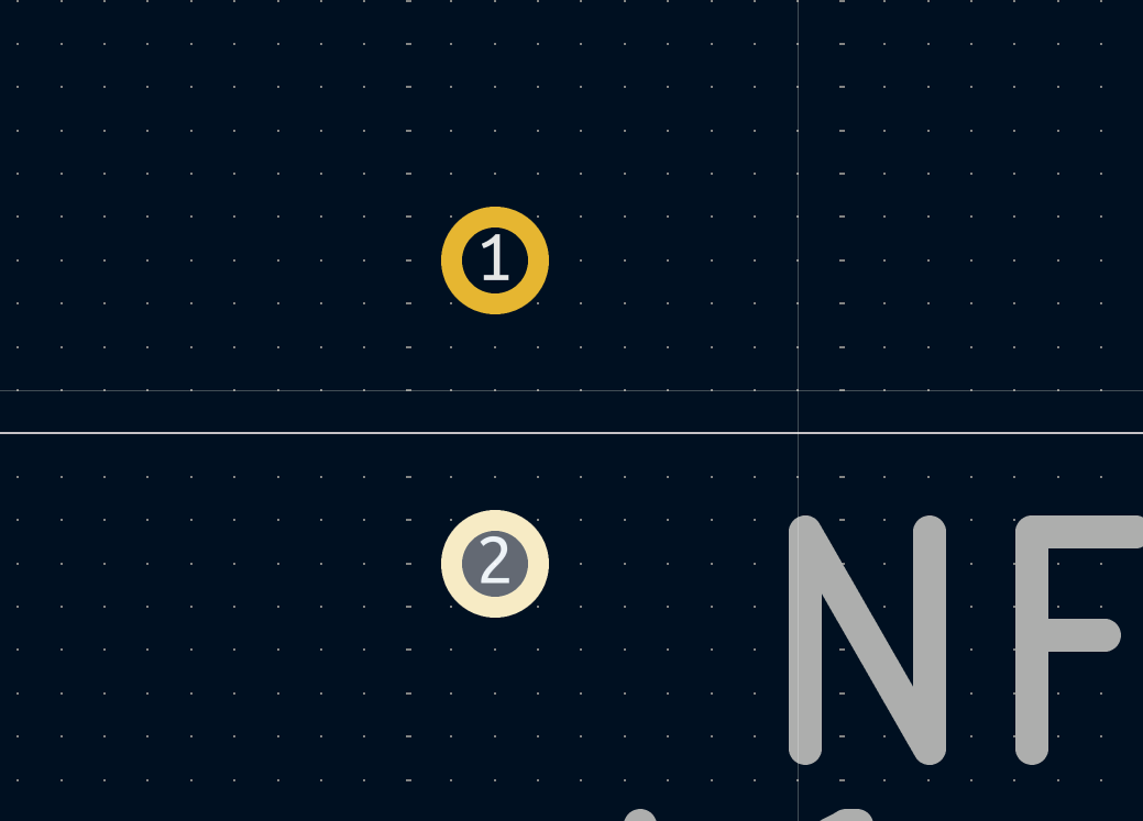
We want to place two pads that are used to connect the rest of the circuit. These pads will be pad 1 and pad 2.
From there we need to lay the actual antenna, using the calculated antenna shape from the previous section we can start creating the antenna using the line and arc tools.
Using example parameters of 35 mm x 25 mm rectangular coil with .2 mm (8 mil) traces with .2 mm (8 mils) gaps with 4 turns we can construct an antenna.
Using the line tool I will draw the outer turn to be the appropriate size. It is recommended to set the grid to an appropriate value to help align your antenna. The start and end point don’t matter very much but will affect the layout. It is recommended to use the center of the copper to measure the length rather than the edges, the difference is too small to make a difference and it makes routing significantly easier.
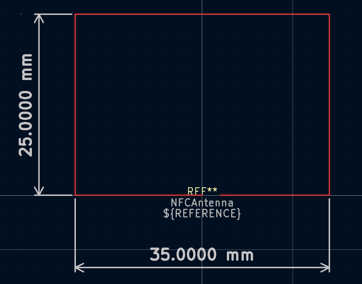
Do not worry about the width of the trace just yet, the only thing to worry about from here is the distance between the turns from center to center, in this case that distance is 16 mils (.4 mm) (Trace Gap + Trace Width). We will place another turn that is inset by that distance. We will repeat this process until all loops are placed. The Grid may need to be changed or the antenna moved to best ensure proper spacing.
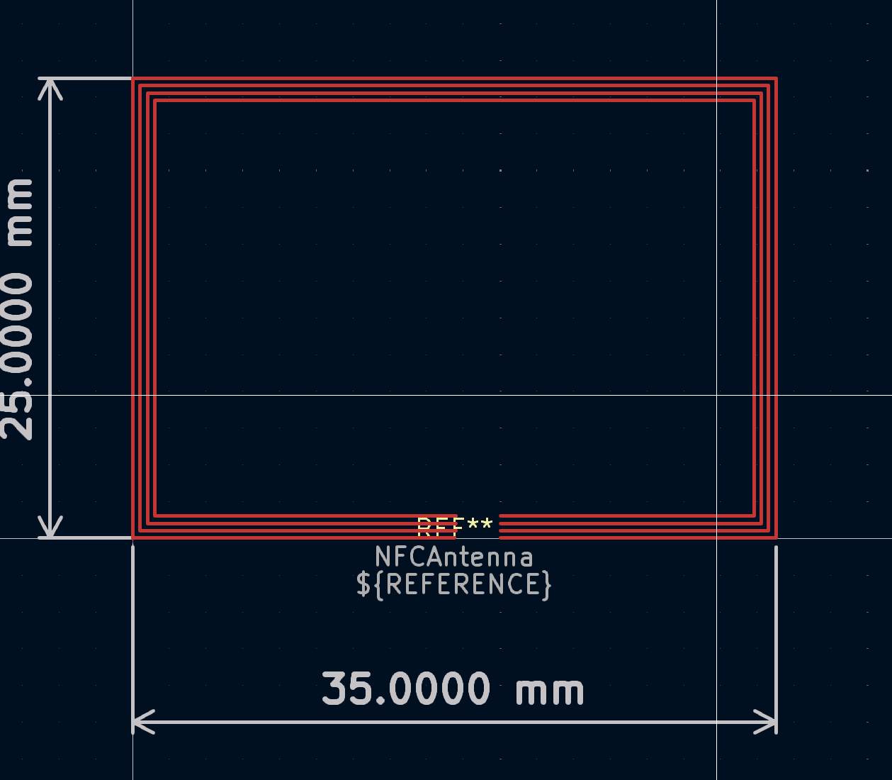
Then the coils can be connected.
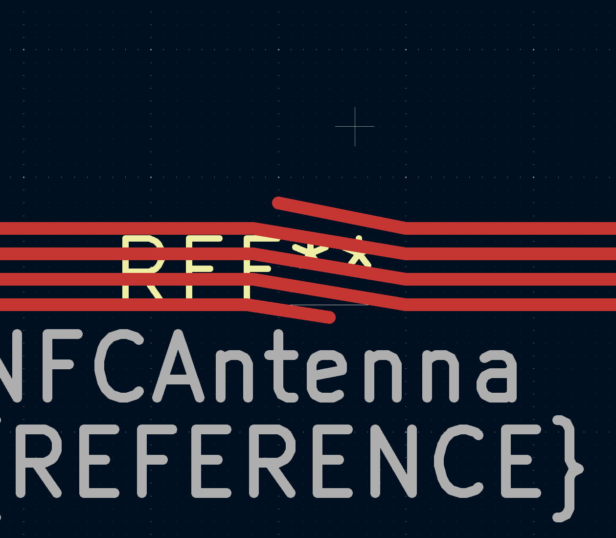
It is recommended to add extenders to the end and beginning to be able to add the pins to the antenna.
Now the trace width needs to be set, to do this click on a trace and press “E”, under width enter the desired width and press “OK”. Repeat this for all segments in the antenna.
Now we need to add the pads and connect them to the traces to that the connect to the end and the beginning with very little space in the x direction as shown.
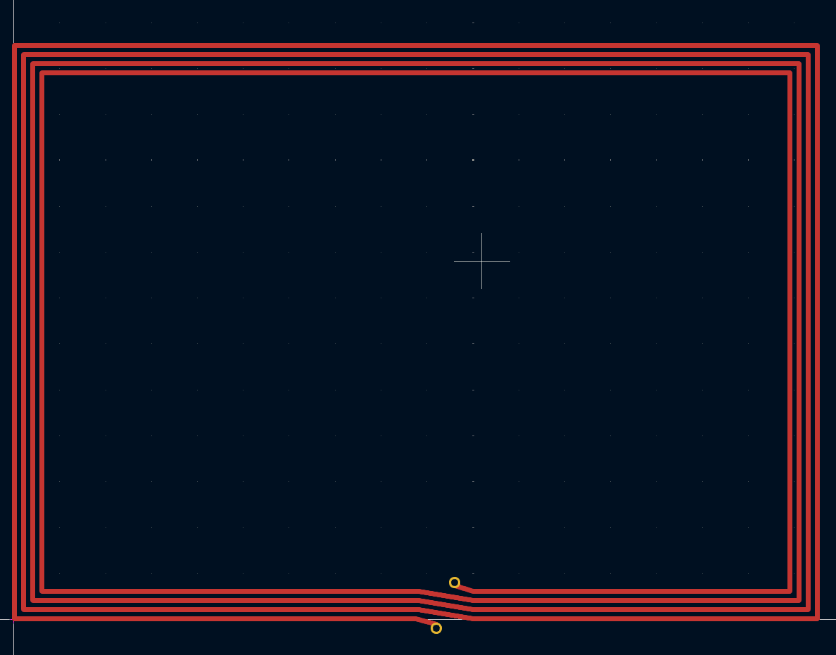
Now you need to tell KiCad that the footprint is supposed to be an antenna by allowing the footprint to have shorts.
Press “E” in the Footprint Editor and navigate to “Clearance Overrides and Settings”
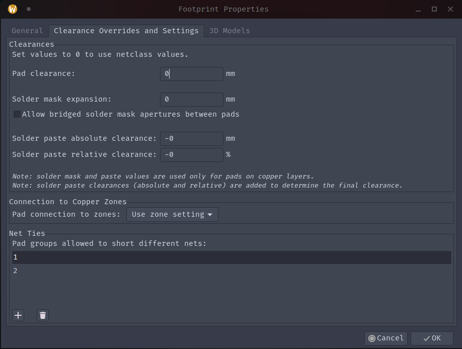
Under the section titled “Net Ties” add “1, 2” in one entry to the list of pad groups. The image above shows what NOT to do.
Once the pads are added then the design is done. Save it to a library (probably a project local one) and assign this footprint to the antenna in the schematic.
While in the schematic, assign the tuning capacitor the correct value. The value of the tuning capacitor should be set so that the resonant frequency of the system lies at 13.56 MHz. Here is some reference material from Ti. and additional notes
A calculator can be seen here. Enter the frequency of 13.56 MHz and the inductance calculated using the antenna calculator. The capacitance provided is the system capacitance required.
The capacitance of the system consists of the on-chip (tuning) capacitance as well as the external tuning capacitor. The sum of these two values is the system capacitance. To find the desired tuning capacitor value subtract the on-chip tuning capacitance (found in datasheet) from the capacitance value calculated earlier. The capacitance value should be in pico Farads (pF).
Set the value of the tuning capacitor accordingly and move to the PCB editor.
Import the schematic in to the PCB and the antenna should appear along with the changes to the tuning capacitor.
Moving Components in to Place
Now that all of the components are on the board we need to move the components to logical places so that they can be connected easily.
It is recommended to place the components outside of the antenna but if it absolutely necessary the other components can be placed inside of the antenna loop.
For example, this would be a reasonably good placement
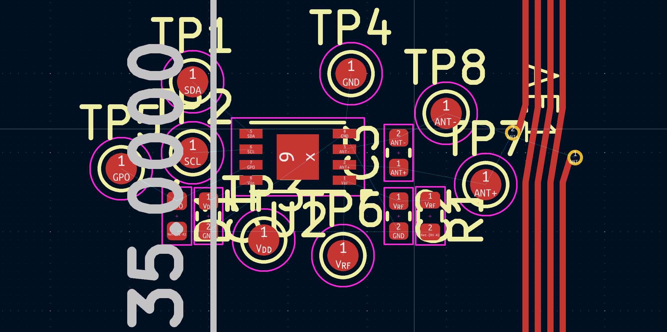
We want to try and reduce rats nest crossover as much as possible. If you have any area of the card dedicated to the electronics on the card, ensure that they are all placed there. We will fix the visual mess with the silkscreen later.
If the antenna is reversed of that you want, you can reverse the symbol in the schematic to flip the connections. This can be done by pressing “Y” on the antenna symbol to flip the component in the Y direction. Once the changes are made, they can be brought to the PCB and your layout will be cleaner.
Connecting the Components
Now that all of the components are on the board and placed approximately where they need to be connected using traces or filled zones.
Select a track width from the drop down, generally the bigger the better, and start connecting pads to one another. Select a via size as well so that if layer changes need to be made they can be. DO NOT ADD A FILLED AREA WHERE THE ANTENNA IS.
Connect all of the pads together, changing layers occasionally if necessary
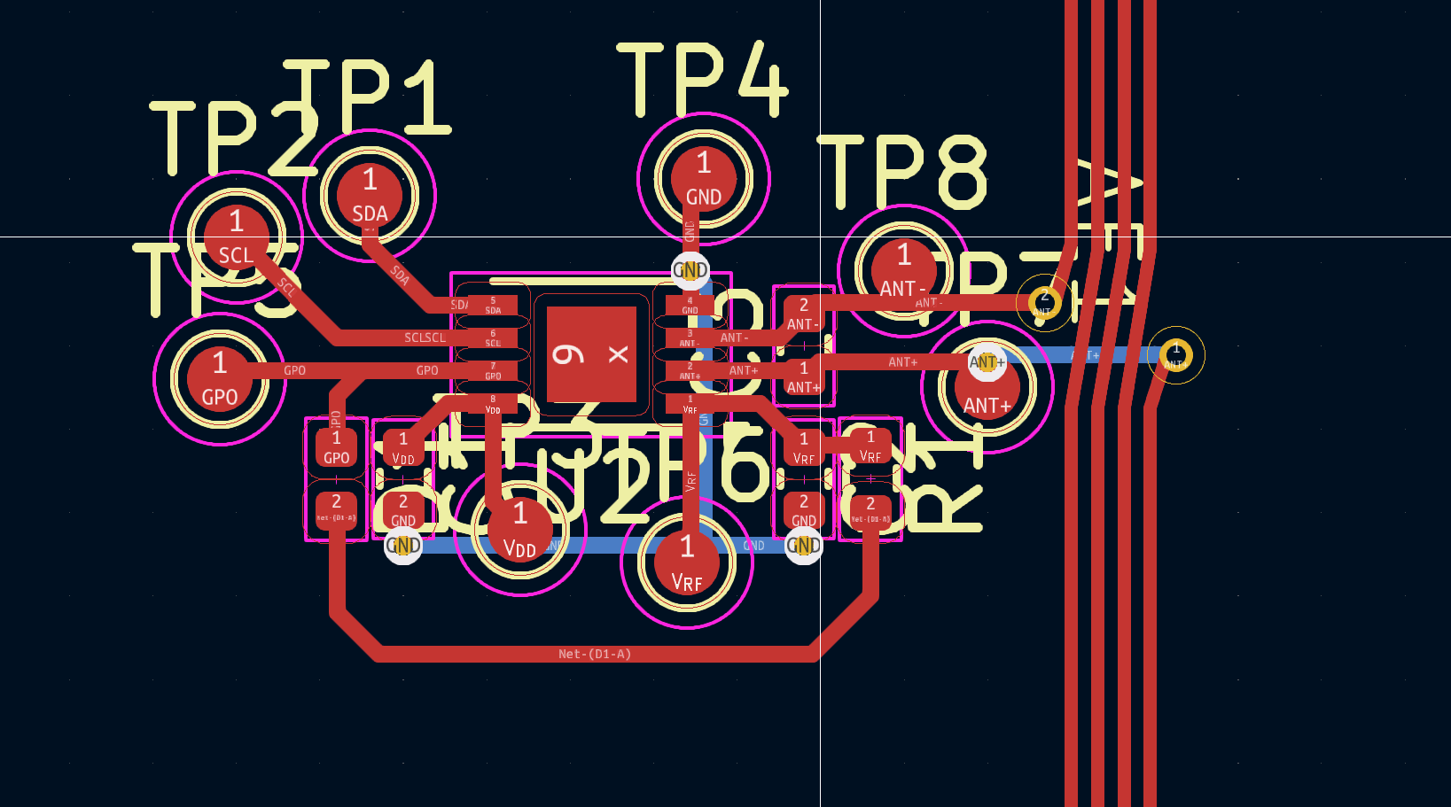
This is all of the connections
Adding Extra Copper
If you want extra logos, decals, or anything else in Copper, now is the time to generate it. It is recommended to use another design tool like Inkscape to generate an SVG file. Those graphics can be imported as in Importing External Graphics to the F.Cu or B.Cu Layer to be easily visible externally.
Adjusting Silkscreen and Solder Mask
Before the board can be manufactured the silkscreen needs to be cleaned up and added too if desired.
Change the Layer to “F.SilkScreen” and we can start moving, deleting, or resizing a lot of the noise in the design.
If you desire you can delete all component designators, this is not recommended but yields the cleanest design possible. The recommended approach is to resize and move the silk screen items so that every item is easily visible.
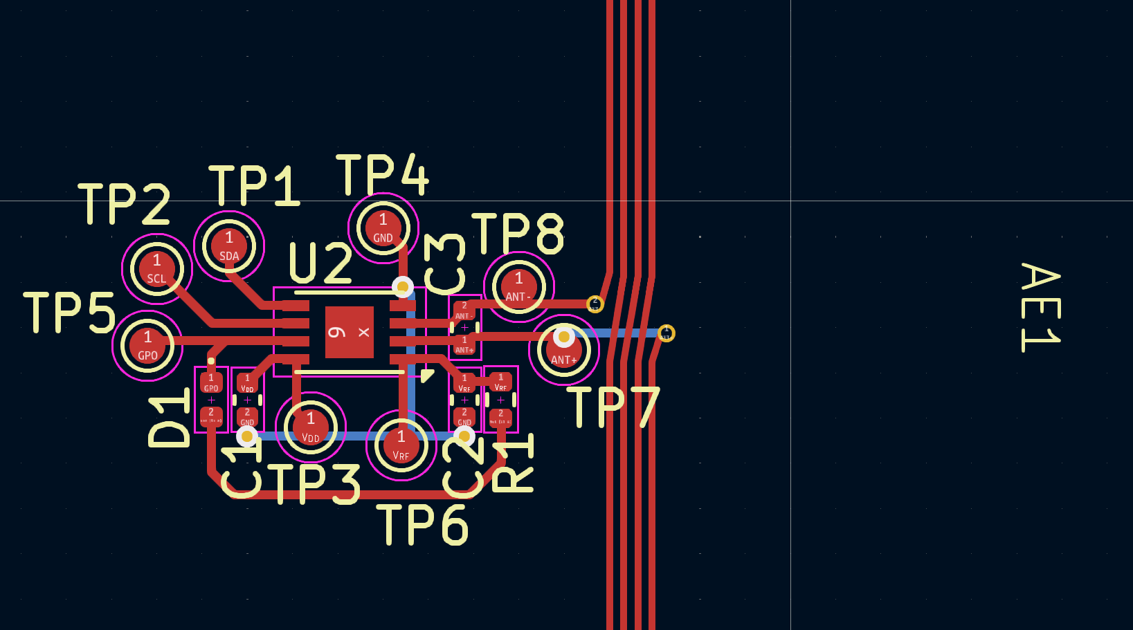
Now that the silkscreen is cleaned up we can add silkscreen of our own which will serve as the marketing material on the card. Things like a QR code, you email, phone number, website, and name would be important to put on this.
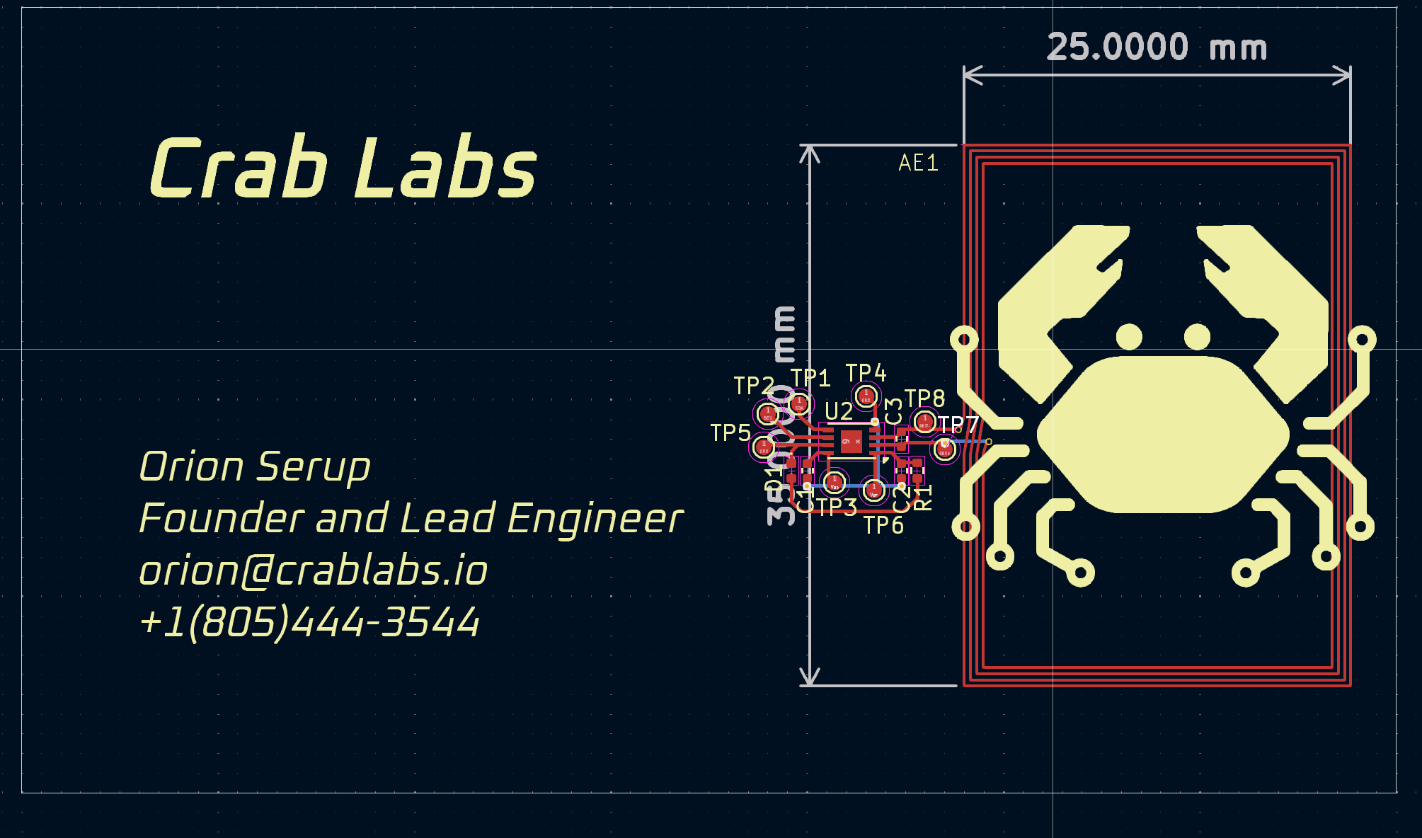
Here is a good example of the front side. It is recommended to add material to both the front and back (F.Silkscreen and B.Silkscreen). It is a good idea to include the NFC logo as well as any other logo or branding that you want as well as any cool designs.
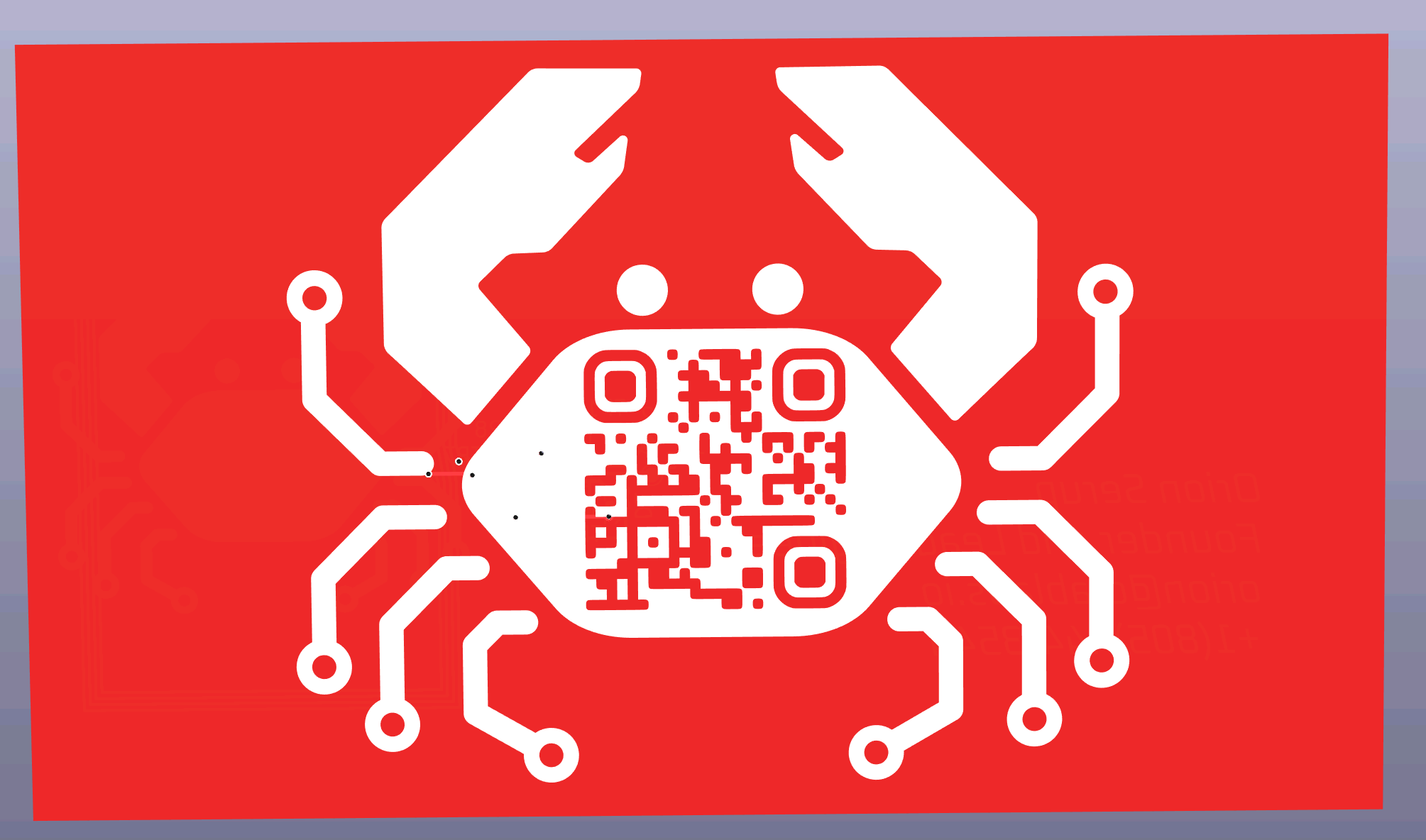

This is what was designed for this tutorial. Make sure to check the look with the 3D viewer.
Checking the Layout
The design needs to be checked for errors or manufacturing issues, this will be done through Design Rules Check or DRC.
In the PCB editor navigate to “Inspect -> Design Rules Checker”
Run the DRC
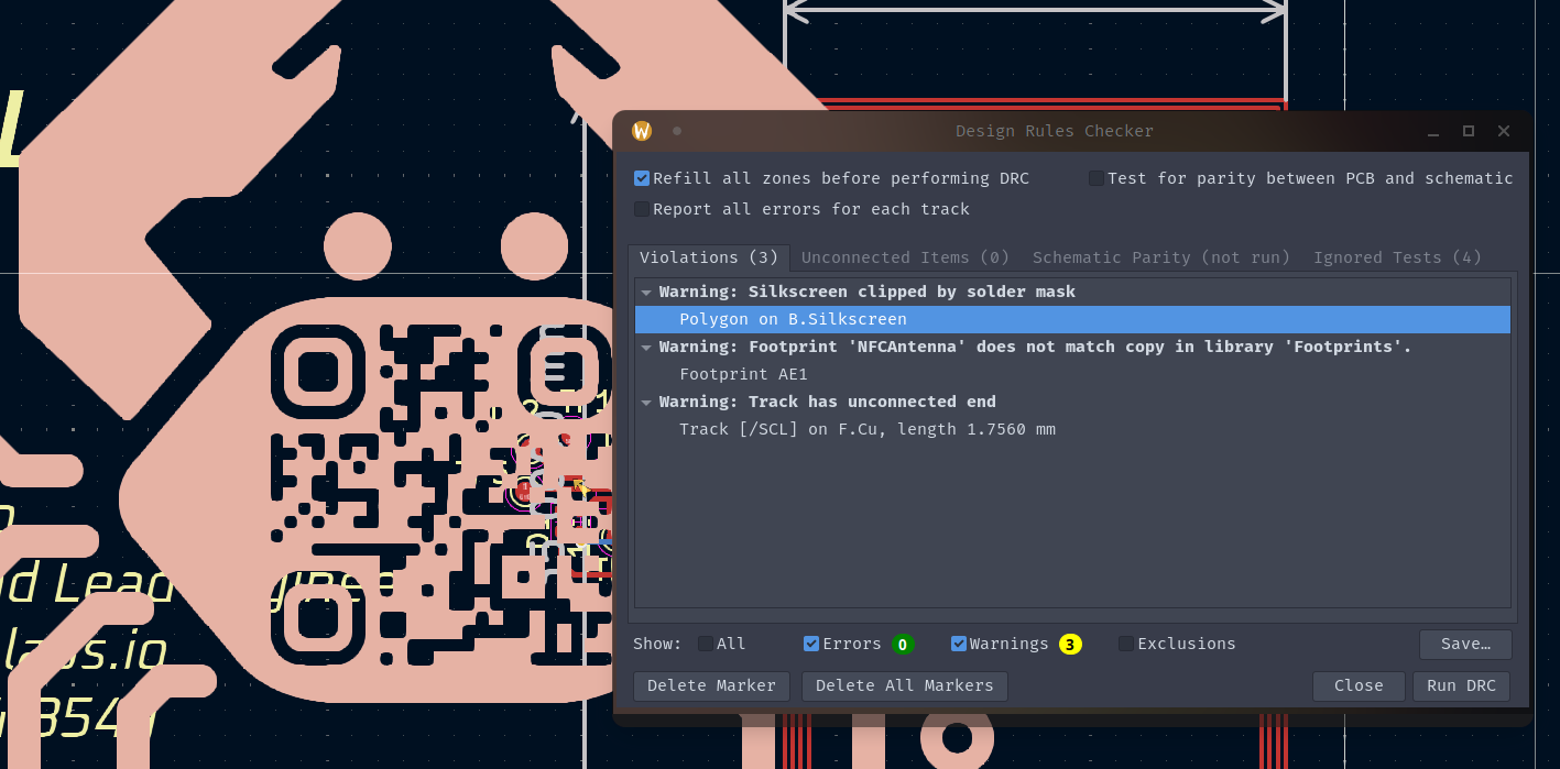
If there are any errors, then address them. Ideally there would be zero warnings and errors, it is recommended to clear all of the errors. Click the violation to pinpoint the location of the offending element.
Ordering the PCB
Once the board has passed DRC, then the board can be sent to be manufactured. The recommended manufacturer for this project is JLCPCB. This tutorial will cover how to order from them, most of the information will be the same between other manufacturers.
Exporting Gerbers
Gerber files are what manufacturers take to manufacture a PCB. They can be generated from the PCB editor.
Navigate to “File -> Fabrication Outputs -> Gerbers”
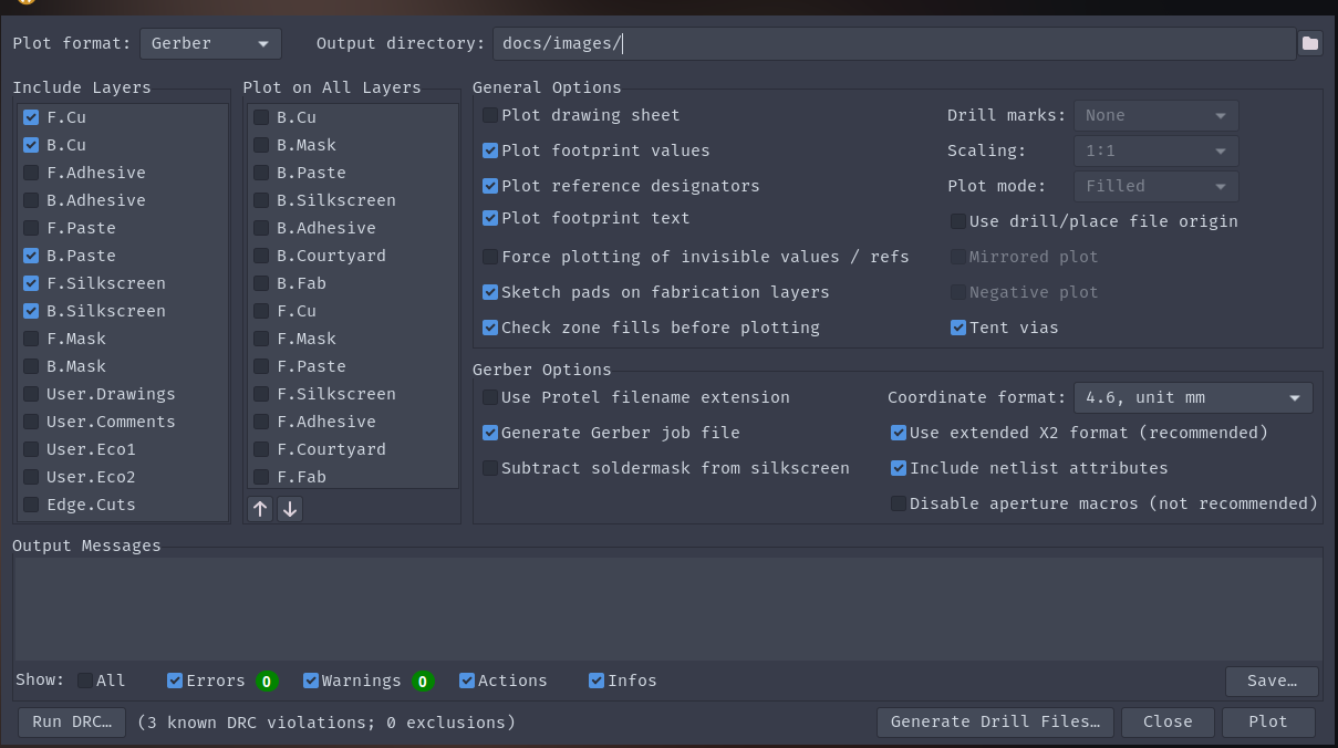
Select an empty directory in a place you know to place the gerber files. Make sure the following layers are selected on the left hand side menu:
- F.Cu
- B.Cu
- F.SilkScreen
- B.SilkScreen
- F.Paste
- B.Paste
- F.Mask
- B.Mask
- Edge.Cuts
- F.Fab
- B.Fab
Press “Plot” and click “Generate Drill Files”. In the drill file menu, set the destination the same as the gerbers and press “Generate Drill File”
Exporting the BOM
The BOM contains all of the parts, their values, as well as their designator (e.g. R1).
From the PCB editor navigate to “File -> Fabrication Outputs -> Bill of Materials”
Save it somewhere memorable and name it something reasonable
Exporting the Position File
The position file contains where each item on the BOM is on the actual board.
From the PCB Editor navigate to “File -> Fabrication Outputs -> Component Placement”
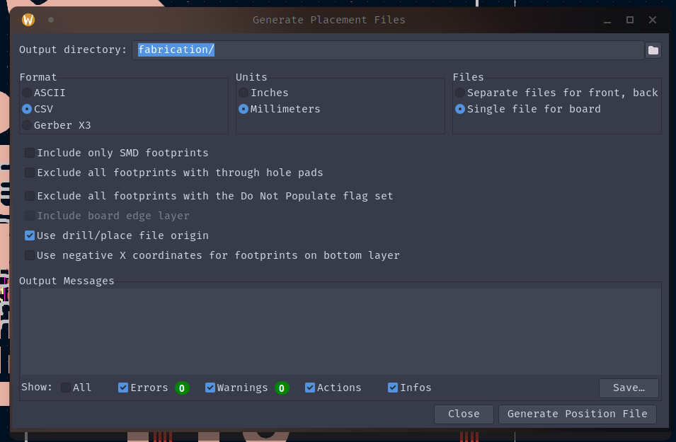
Make sure that the output is set to a memorable location with a memorable name.
Set the format to CSV, with a Single File for the Board in Millimeters.
Press “Generate Position File” and we are done generating output files
Placing the Order on JLCPCB
Once all of the files are ready we can open up JLCPCB.
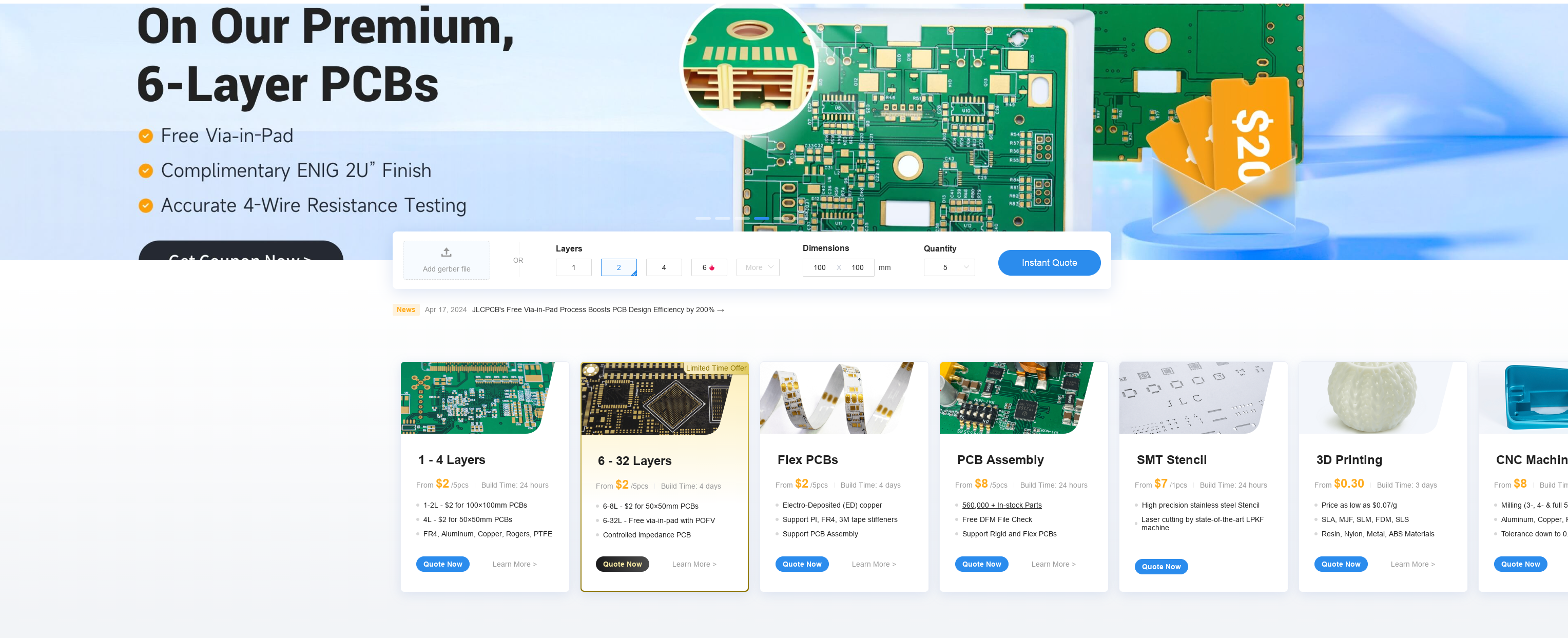
In order to order the PCBs we need to zip the folder with the gerbers and drill files and upload it where indicated.
If the files were properly generated it should look something like this
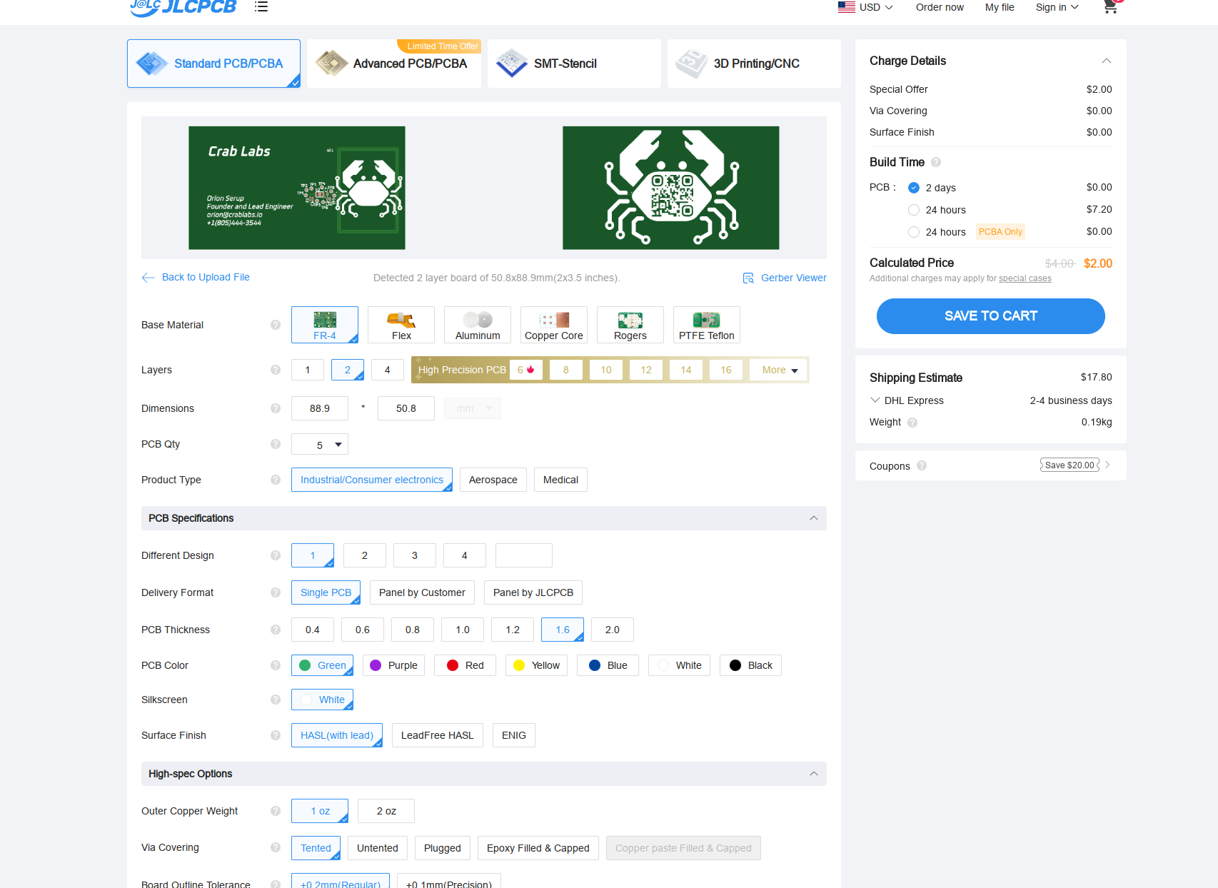
Here is where we can customize the look of the PCB. Pick a color.
If you plan on assembling the PCB yourself then you can proceed to checkout and skip the rest of this section.
To get your PCB assembled, navigate to the bottom of the page and select “PCB Assembly”
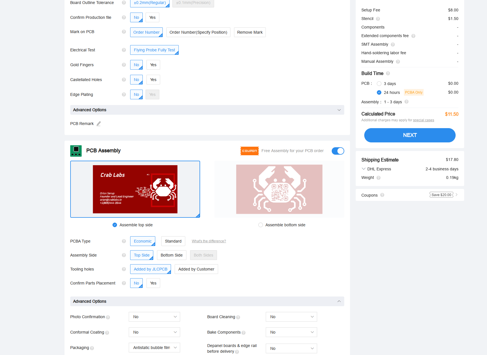
Select “Economic” and whichever sides you have the parts on (likely the top).
Allow JLC to add tooling holes and make sure to mark “Confirm Parts Placement”
Press “Next” on the right hand side. Once you click through and verify the gerbers look right it will take you to this screen
Upload your BOM. Before you can upload the Position file we need to modify it slightly so that JLC will accept it. Open the CSV file and change “Pos X” to “Mid X”, “Pos Y” to “Mid Y” and “Rot” to “Rotation” and then upload where indicated.
From there JLCPCB will find parts that match your criteria.
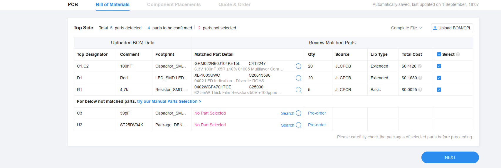
If JLC can’t find a part that aligns with what you have you will need to find it yourself.
Click on search next to the item and put in key words or values.
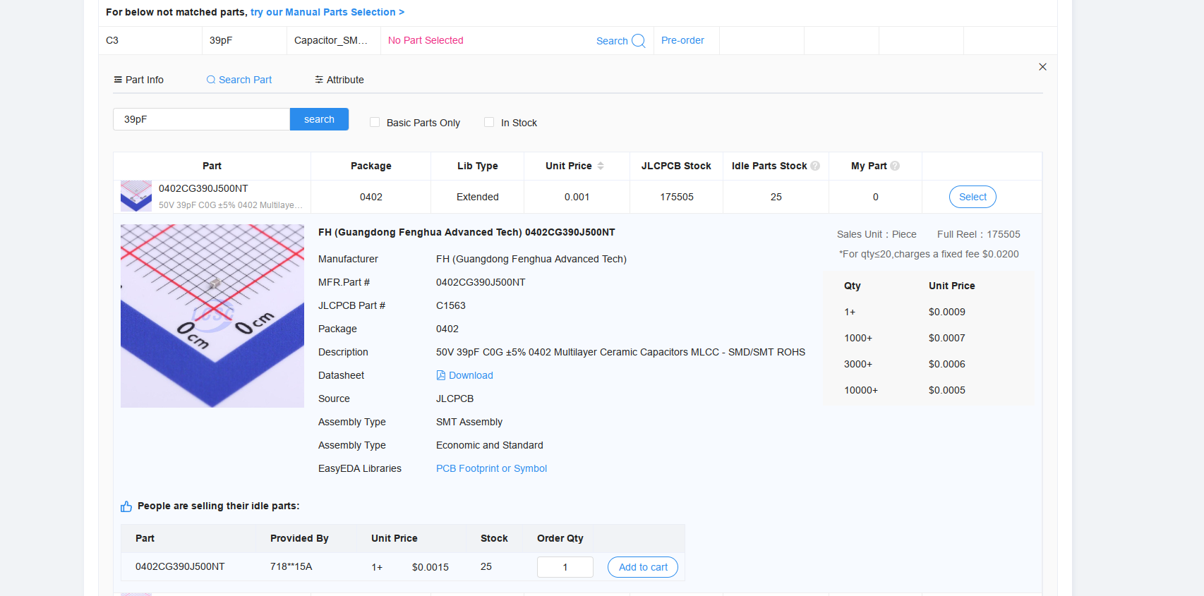
For this tuning capacitor, you may not be able to find the exact value in the exact package. In that case play around and try to find a value as close as possible.
As for the NFC tag IC, it is important to find something with the right footprint. I would recommend inputting in just the few characters of the tag name and searching from there.
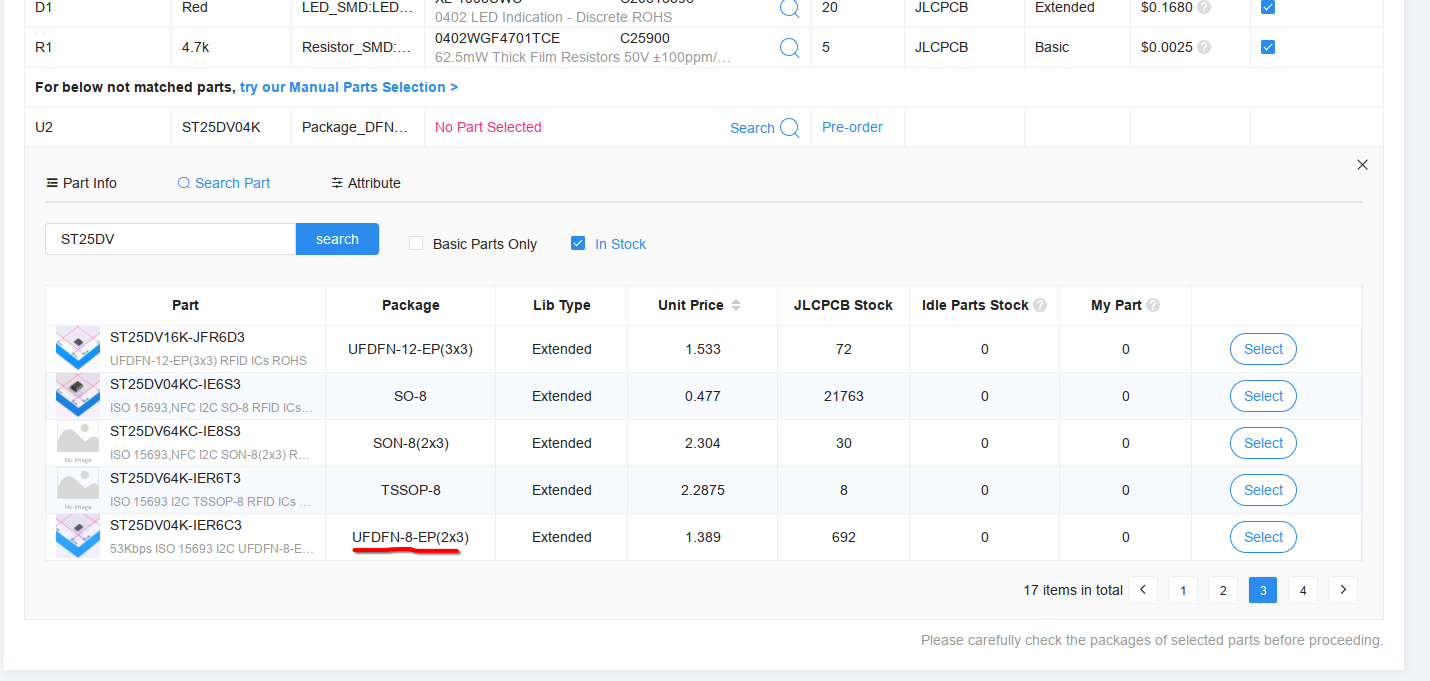
Once all of the parts have been selected click next. This will take you to the preview screen to see how the board will look populated.
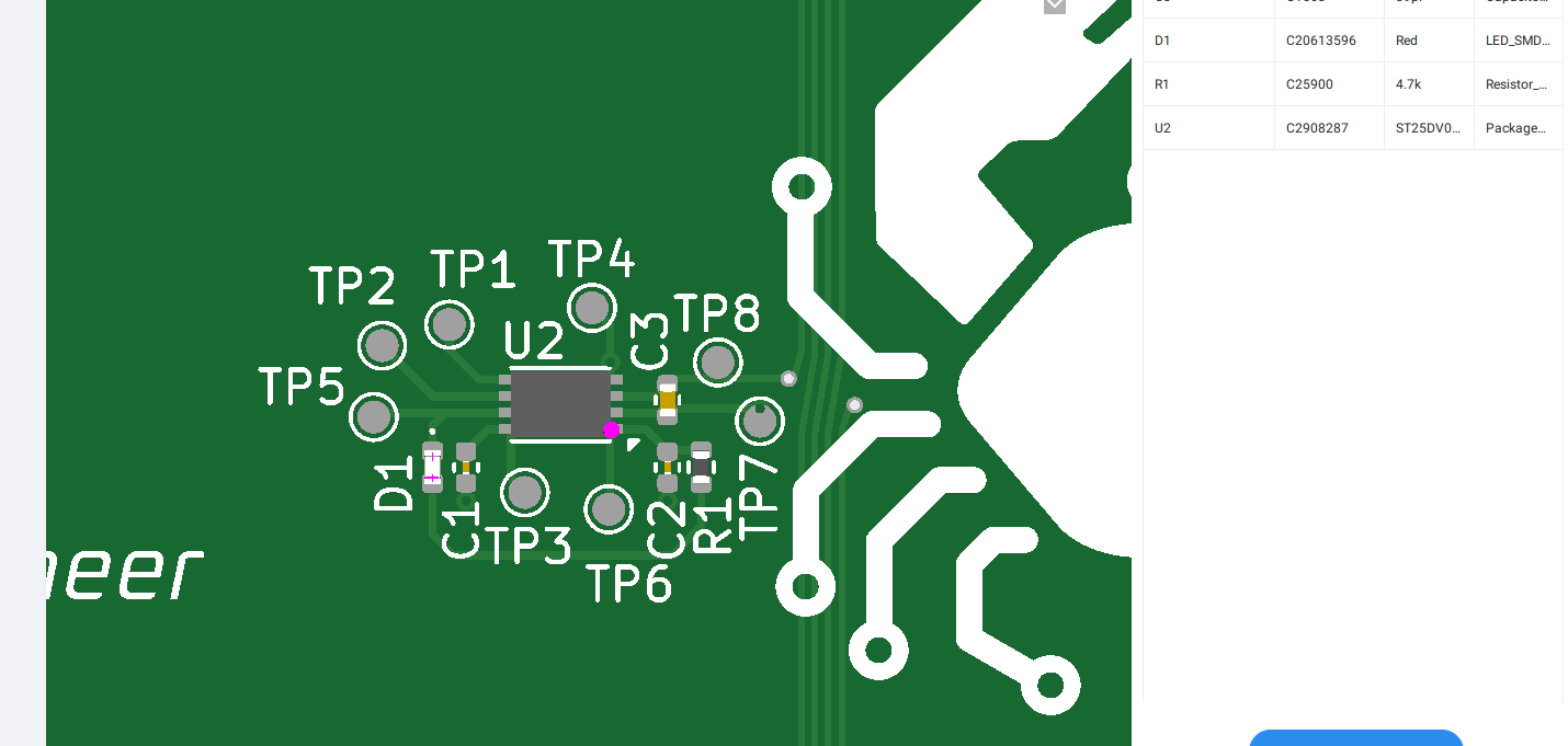
If you see that a part doesn’t fit or doesn’t look right (such as the capacitors above) go back to the part select screen and adjust the offending parts.
If a part is rotated or positioned incorrectly, it can be corrected by clicking on the item, dragging it and/or rotating it using the built in tools.
Once all of the parts are corrected the parts should align and look good, similar to as shown below
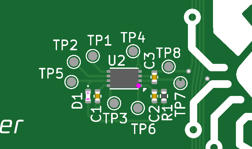
Click next and save to cart and order. They will be on the way in a few days.
Assembling the PCB
If you opted to fully or partially assemble the components, good luck. Make sure that parts are oriented and placed correctly. Here is a video which will likely help you.
Testing the PCB
Once the PCB has arrived it is now time to test to ensure that the NFC tag works as expected.
Download the “NFC Tools” app from the App Store or Google Play Store / F-Droid.
Open the app, turn NFC on if it wasn’t on and approach the PCB where the antenna is.
The PCB works if Tag information is displayed on the screen as shown here
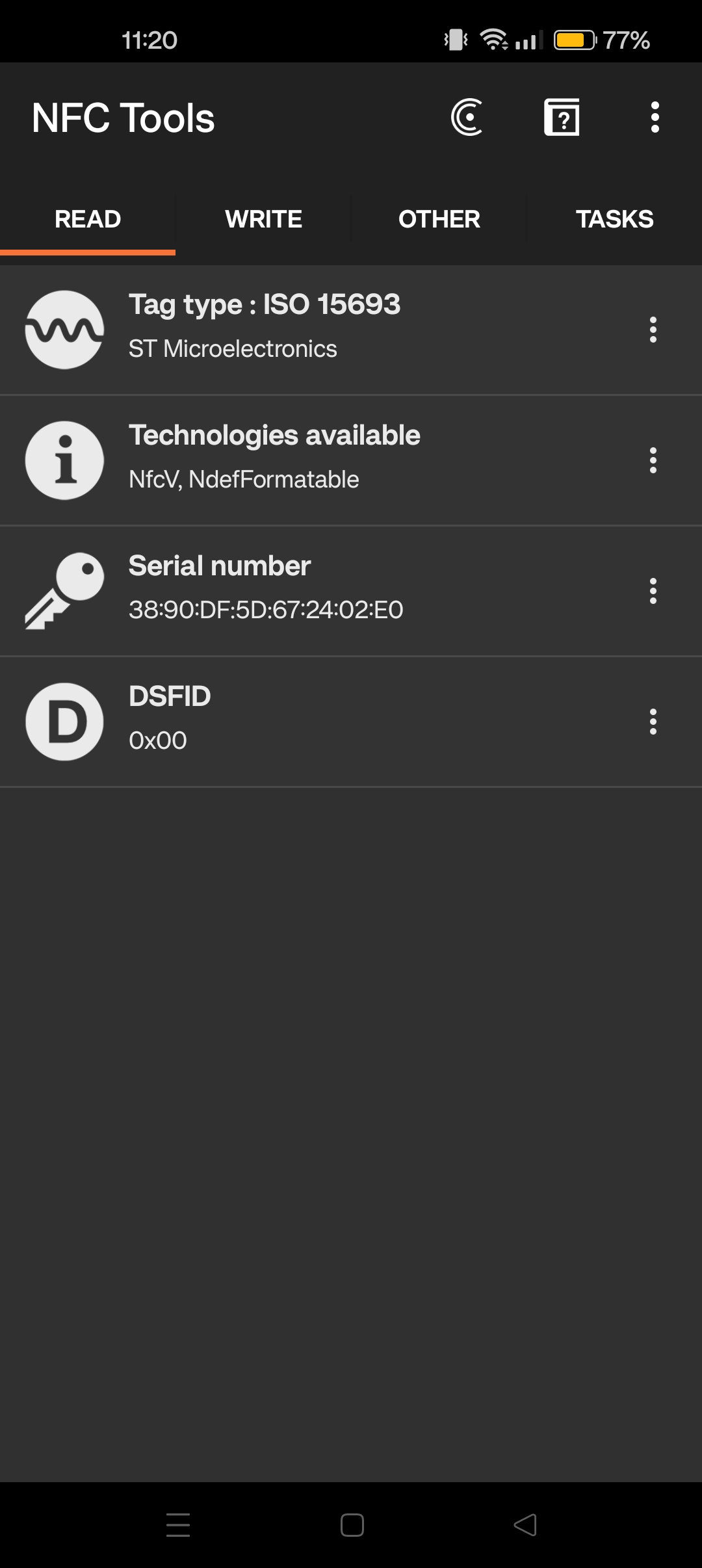
If information isn’t shown the most likely issues are as follows:
- Improper tuning capacitor value
- Bad Antenna
- Short or Discontinuity
Writing the Information on the Tag
To write an entry on to the device navigate to the “Write” tab in the App.
Click “Add Record”
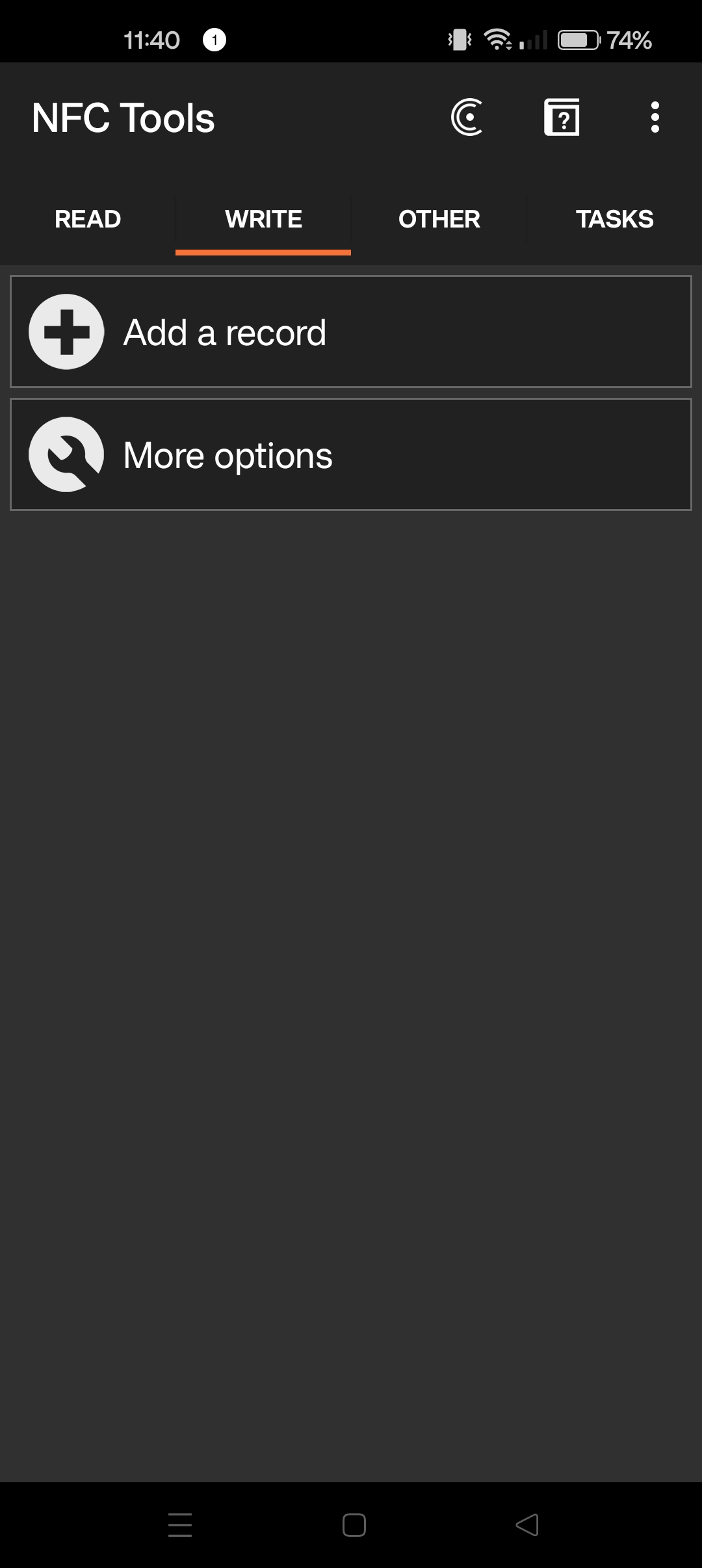
You can add any kind of record that you want, a URL is the most universally recognized and thus is the recommended data to store.


Enter your URL
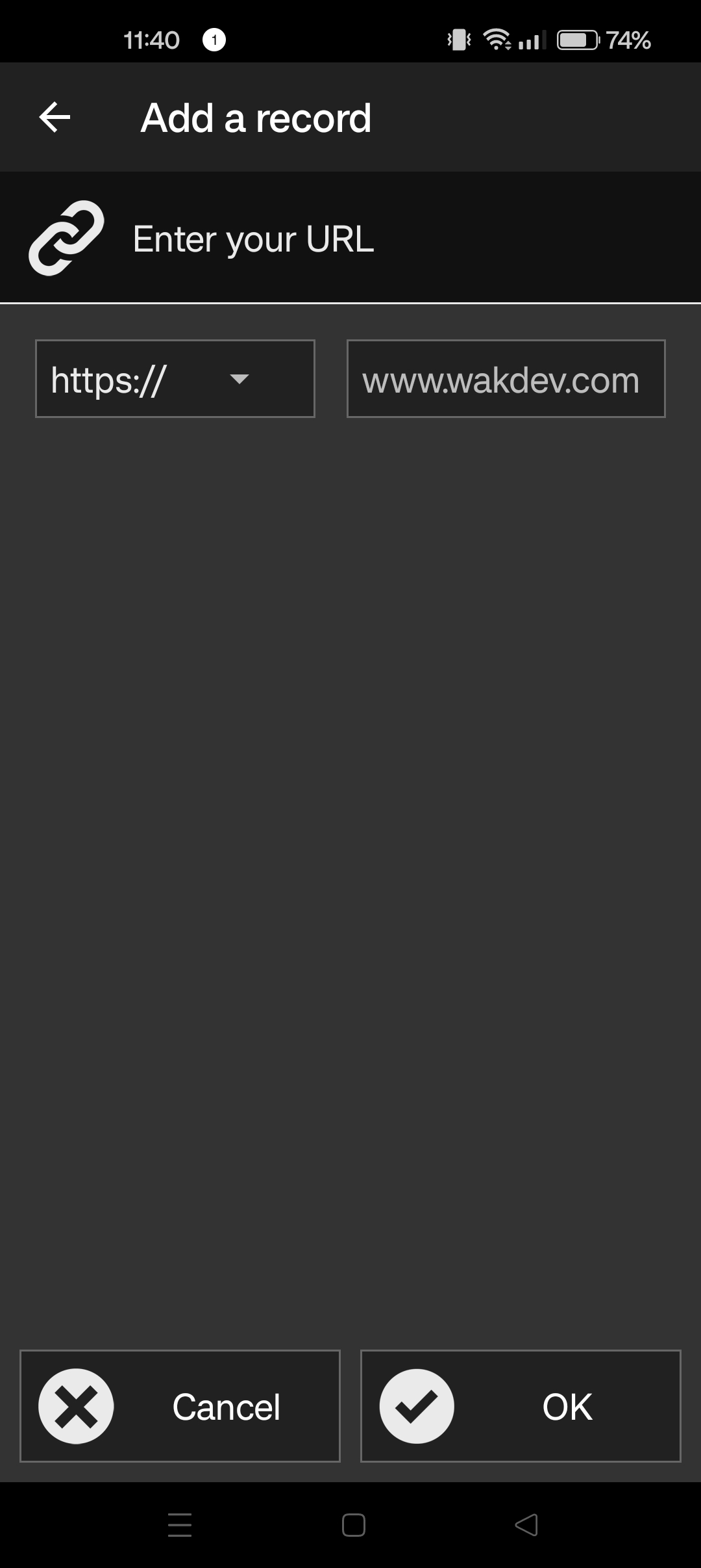
You will then be taken back to the write page
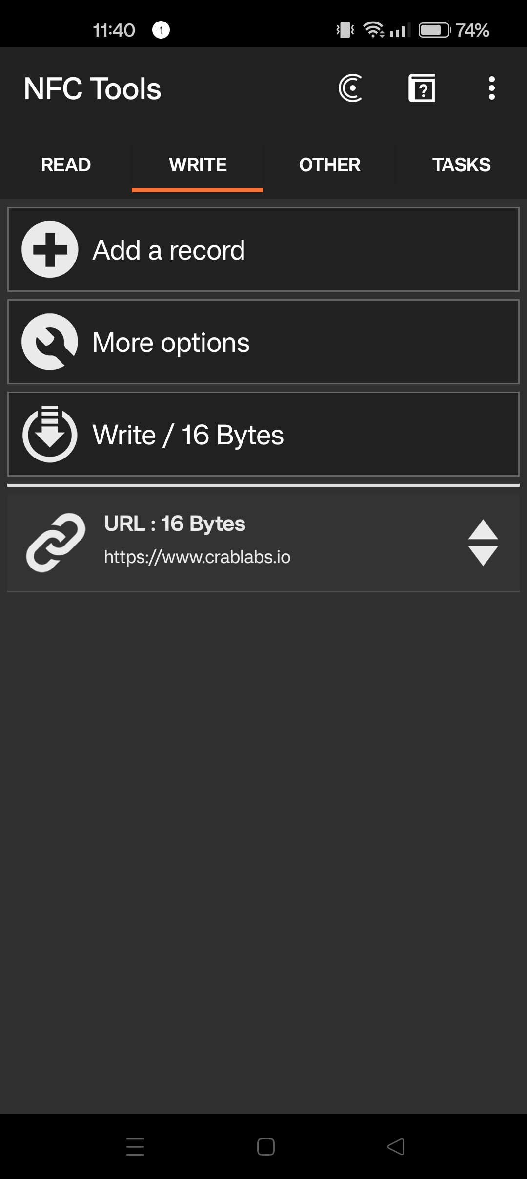
You can add additional records as required or desired by repeating the previous process. Write them to the device by clicking “Write”
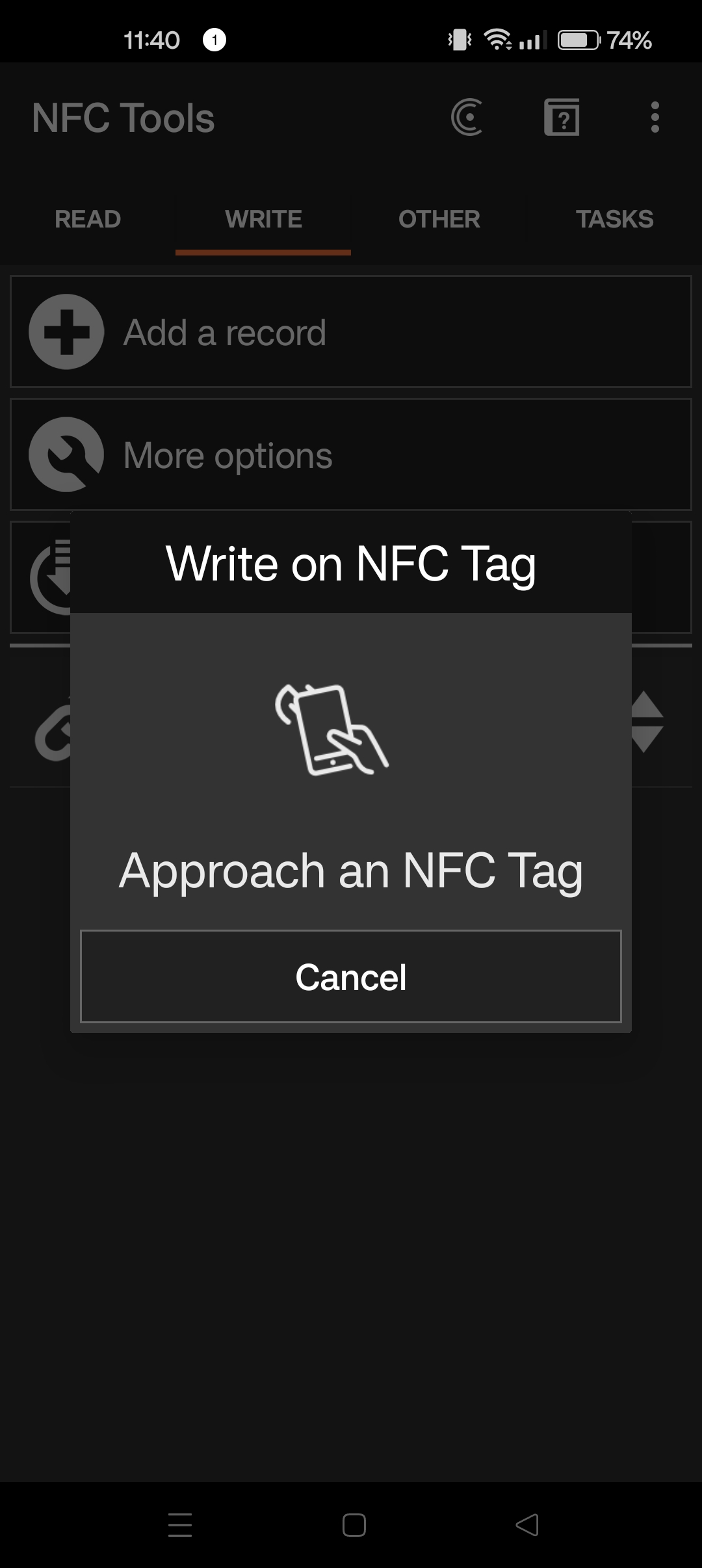
Approach the tag. If the write was successful you will see this:
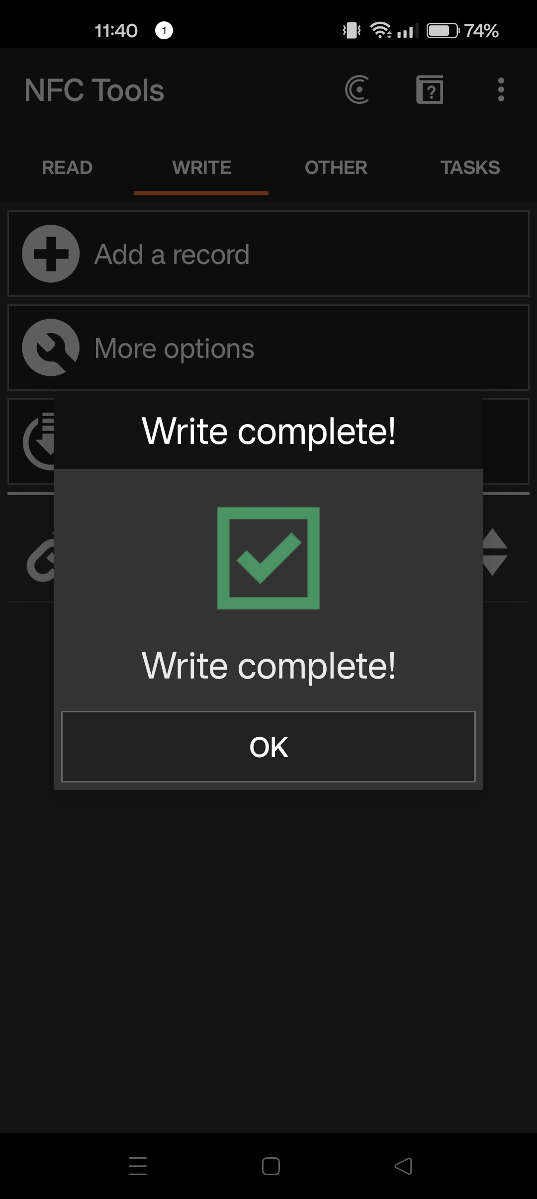
If the write does not complete successfully, the following issues may be the culprit:
- Bad Antenna/Tuning Circuitry
- Movement of device while trying to write
- Records are larger than the amount of storage on the tag
- Device out of range
